Hello,
My customer has problem about ADC of TM4C123GH6PGEI.
Here is his code for the ADC. This code uses same analog input for easy explanation.
uint32_t ui32Value[8] = {};
void
initADC{
//Port enable
ROM_SysCtlPeripheralEnable(SYSCTL_PERIPH_GPIOE);
ROM_SysCtlPeripheralEnable(SYSCTL_PERIPH_GPIOK);
// Configure the pins to be used as analog inputs.
ROM_GPIOPinTypeADC(GPIO_PORTE_BASE, GPIO_PIN_2 | GPIO_PIN_3));
ROM_GPIOPinTypeADC(GPIO_PORTK_BASE, GPIO_PIN_0 | GPIO_PIN_1 | GPIO_PIN_3);
//ADC clock speed = 1MSPS
ROM_SysCtlADCSpeedSet(SYSCTL_ADCSPEED_1MSPS);
// Enable the ADC peripherals
ROM_SysCtlPeripheralEnable(SYSCTL_PERIPH_ADC0);
//Reset the ADC peripherals
ROM_SysCtlPeripheralReset(SYSCTL_PERIPH_ADC0);
//Wait "READY"
while(!ROM_SysCtlPeripheralReady(SYSCTL_PERIPH_ADC0));
// Select the external reference for greatest accuracy.
ROM_ADCReferenceSet(ADC0_BASE, ADC_REF_EXT_3V);
// Initialize both ADC peripherals using sequencer 0 and processor trigger.
ROM_ADCSequenceConfigure(ADC0_BASE, 0, ADC_TRIGGER_PROCESSOR, 0);
ROM_ADCSequenceStepConfigure(ADC0_BASE, 0, 0, ADC_CTL_CH2);
ROM_ADCSequenceStepConfigure(ADC0_BASE, 0, 1, ADC_CTL_CH2);
ROM_ADCSequenceStepConfigure(ADC0_BASE, 0, 2, ADC_CTL_CH2);
ROM_ADCSequenceStepConfigure(ADC0_BASE, 0, 3, ADC_CTL_CH2);
ROM_ADCSequenceStepConfigure(ADC0_BASE, 0, 4, (ADC_CTL_IE | ADC_CTL_END | ADC_CTL_CH2));
ROM_ADCSequenceEnable(ADC0_BASE, 0);
ROM_ADCIntClear(ADC0_BASE, 0);
}
void
Acquire(){
// Trigger the sample sequence.
ROM_ADCProcessorTrigger(ADC0_BASE, 0);
// Wait until the sample sequence has completed.
while(!ROM_ADCIntStatus(ADC0_BASE, 0, false));
ROM_ADCIntClear(ADC0_BASE, 0);
// Read the value from the ADC.
ROM_ADCSequenceDataGet(ADC0_BASE, 0, ui32Value);
}
void
SysTickIntHandler(void)
{
Acquire();
}
void
main{
ROM_FPUEnable();
ROM_FPULazyStackingEnable();
//80MHz PLL Clock
ROM_SysCtlClockSet(SYSCTL_SYSDIV_2_5 | SYSCTL_USE_PLL | SYSCTL_XTAL_20MHZ | SYSCTL_OSC_MAIN);
//ADC Configuration
initADC();
//SysTick Configuration
ROM_SysTickPeriodSet(ROM_SysCtlClockGet() / 100);
ROM_SysTickIntEnable();
ROM_SysTickEnable();
ROM_IntMasterEnable();
while(true)
{
}
}
Problem is similar to errata ADC#14 of below.
http://www.tij.co.jp/jp/lit/er/spmz849b/spmz849b.pdf
The first two ADC samples are lower than expected.
We expect 0x24E for VADCIN which is DC signal.
But First two are 0x230 and the third ~ the fifth are almost 0x24E.
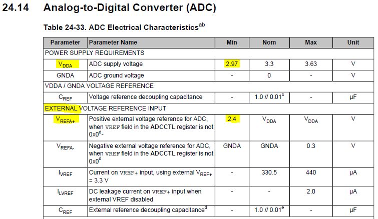
He uses External voltage reference (VREF+ = 2.5V,VREFA- = GNDA).
External reference decoupling capacitors are 1.0μF and 0.01μF in parallel.
I hope you can help us.
Best regards,
Sugita