Other Parts Discussed in Thread: BOOSTXL-DRV8301, ENERGIA, LM120
Dear Texas Instruments,
I've been looking into using the BoosterPack standard as the expansion port for a product we are developing. The problem is the standard needs some work.
I've come across two conflicting BoosterPack standards:
1) http://www.ti.com/ww/en/launchpad/dl/boosterpack-pinout.pdf (last updated Sept 1, 2013)
2) http://processors.wiki.ti.com/index.php/BoosterPack_Standards_and_Design_Guide (last updated Oct 3, 2013)
The second link is the most recent and most detailed, but also has OBSOLETE written somewhat down the document. Is there some documentation that describes the dimensional aspects that is not labelled obsolete.
I can tell that the standard evolved rather than being planned.
For instance, the second document states "BoosterPacks should not extend more than 0.350 inches above the center of the top BoosterPack interface pin", yet all the BoosterPacks that I've looked at violate this "requiremnt". For instance, the BOOSTXL-DRV8301 Motor Drive BoosterPack extends 1.200 inches and the Sensor Hub BoosterPack for Tiva™ C Series LaunchPad extends 0.500 inches.
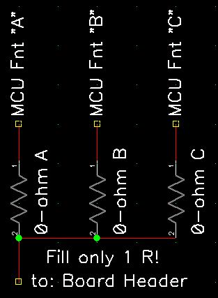
The standard allows boards to extend below the 20/40 pins to include two extra ground and an extra VCC pin, but non of the boards use this since then they would cover the Tiva launchpad user buttons.
Moving onto the electrical side it's a minefield.
The first link has pin A6 as Analog In, while the second link has pin A6 as GPIO. Similar problems on pins A9, A10, B6 and B7.
Pins B4 has been "lost" to various changes which is a big deal when you want to maximise what you can get from 40 pins.
Pins B6 and B7 have changed from being I2C to SPI. This has created an interesting mess for the Tiva Launchpad. It shorts GPIO ports PB7 and PD1 together and GPIO ports PB6 and PD0 together. This is to bring both I2C and SPI to BoosterPack pins B6 and B7, so two microcontroller pins are "lost". Interestingly the PD0/PB6 combination appear on BoosterPack pin C3 and PD1/PB7 combination appear on BoosterPack pin C4, which means you cannot use these pins for analog input and I2C/SPI at the same time.
Even the latest TM4C129x Development Board is affected with links to swap pins around.
TI, when deciding on alternate GPIO functions, it pays to put I2C SDA on the same pin as SSInXDAT0/SIMO and I2C SCL on the same pin as SSInXDAT1/SOMI. For the TM4C129XNCAD microcontroller, asused on te TM4C129X Development Board, there where two intances of this, but one instance swpaped aroudn, which neciessited the links on the development board. Would be good to put this on a microcontroller pinout checklist.
Dear Texas Instruments, it would be good to resolve the issues with the standard and put out a single official document.