Hello!
I'm using TI Tiva C TM4C123GH6PM on the Tiva C launchpad to drive an AD9850 DDS chip. Programming is done in Code Composer Studio 5.5. My clock frequency is 80 MHz.
My basic workflow is right now relatively simple:
I have a main function and at its beginning I set up TM4C's peripherals and reset the AD9850. The peripherals I use are GPIO ports B,E and F via the AHB. I also use the ADC0 and FPU.
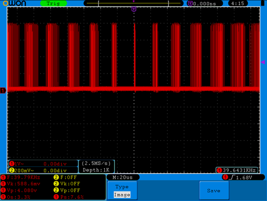
Next comes a loop in which I sample the ADC, calculate settings for the AD9850 and then transfer them using GPIO ports. The calculation and transfer part is constant an takes around 10.4 microseconds. I confirmed this by having a pin go high and then low at the end of the data transfer.
What is problematic is the part where I'm waiting for the ADC to finish. The time it takes for it to do conversion does not seem to be constant.
Here's code I used to set up the ADC:
ROM_SysCtlPeripheralEnable(SYSCTL_PERIPH_ADC0);//Pin is PD1=>channel AIN6
ROM_ADCHardwareOversampleConfigure(ADC0_BASE, 64);
//Averages 64 samples and stores them in one FIFO slot,
//has apparently no effect on the conversion time, same results when disabled

HWREG(ADC0_BASE+ 0x038) = 0x40;//This enables hardware dithering


ADCSequenceConfigure(ADC0_BASE,3,ADC_TRIGGER_PROCESSOR,0);
//Uses ADC0, sequence 3=>FIFO with length of one, highest prioroty
ADCSequenceStepConfigure(ADC0_BASE,3,0,ADC_CTL_CH6|ADC_CTL_IE|ADC_CTL_END);
//First and last step, selects ADC0, sequence 3, step zero, channel 6,
// enables interrupt and ends sequence
ADCSequenceEnable(ADC0_BASE,3);
//Enables sequence
Here's the code I'm using to get the ADC data and toggle a pin when it's done:
ROM_ADCIntClear(ADC0_BASE, 3);//clears interrupt flag

while(!ROM_ADCIntStatus(ADC0_BASE, 3, false))//Waits for ADC to finish converting
{//Busy wait to be replaced with an ISR at some point
}
ROM_ADCSequenceDataGet(ADC0_BASE, 3, adcData);
//adcData pointer to memory location GPIOPinWrite(GPIO_PORTE_AHB_BASE, GPIO_PIN_1, 2);
GPIOPinWrite(GPIO_PORTE_AHB_BASE, GPIO_PIN_1, 0);
My idea is to later on trigger ADC from a timer interrupt and then do the data processing in ADC's interrupt, but before that, I want to understand what exactly is happening here.
Here's an image of the pin I'm wiggling when the ADC finishes: