This thread has been locked.

If you have a related question, please click the "Ask a related question" button in the top right corner. The newly created question will be automatically linked to this question.

EPI External FIFO read problem

Hello I am Using TIVA 129X development Board 

I am using code Provided from this post

http://e2e.ti.com/support/microcontrollers/stellaris_arm/f/471/t/167420.aspx

I am having problem with this code It just reads for 8 Count after every 

EPINonBlockingReadGet8(EPI0_BASE, 1024, g_pucBuffer);

Lets say if I am Putting this in series of read

EPINonBlockingReadGet8(EPI0_BASE, 100, g_pucBuffer);


It just gives me 8 count of read not reading the whole 100 counts.


Tushar

  • Hi Tushar,

    In the code example given, there is a while loop around the EPINonBlockingReadget8, do you have that implemented. Please note that the NBRFIFO is 8 locations deep. So if the read is done very fast, it will empty before it is filled up. In the function prototype, it is a while loop which checks for the count decrementing to 0 and RFIFOCNT register indicating that there is at least 1 unit of data in the NBRFIFO. If either of them is false it will exit.

    Regards

    Amit

  • Hello Amit,

    I just figured that out by inserting delay between two read function I was able to get data.

    but is there any work around with this API because my buffer string every time points to starting address and I cannot see Data for more than 8 counts. I want to load the string to a value of 1024 counts.

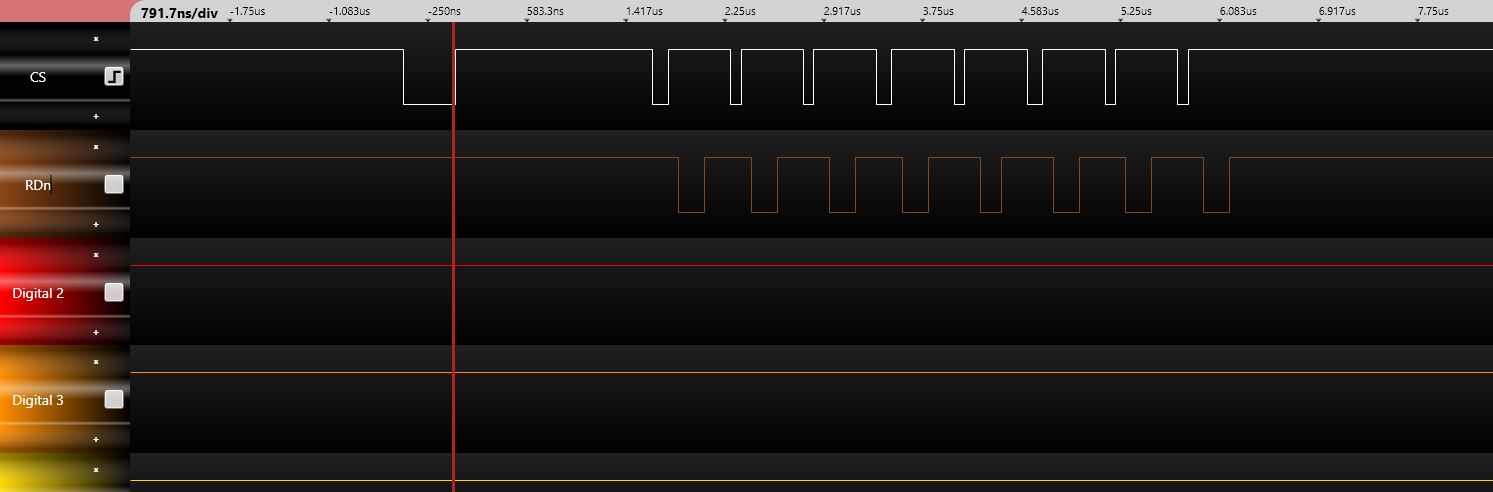
    And if I view Chip Select Signal in Logic Analyzer it is not 50% duty cycle with Read Enable also not align.

    I don't have the Snapshot of this signal now but I will post it tomorrow.

    I am working with TIVA 129X development Board CPU running at 120MHz frequency

    Regards,
    Tushar

  • Hello Tushar,

    You can use the Interrupt to notify you application that data is available in the NBRFIFO and read it instead of using Delay. This way you can make sure that you wait till the size of transfer is not reached and then proceed. Also it will frequency proof your application if you change the System Frequency as the delay will need to be changed.

    Regarding the CS aspect, I would need info on the configuration of EPI and the signals.

    Regards

    Amit Ashara

  • Amit,

    This is the Code for EPI Configuration.

    int main(void) {

    uint8_t ulReadSize, ulLoopCount;

    //
    // Run from the PLL at 120 MHz.
    //
    ui32SysClock = SysCtlClockFreqSet((SYSCTL_XTAL_25MHZ |
    SYSCTL_OSC_MAIN |
    SYSCTL_USE_PLL |
    SYSCTL_CFG_VCO_480), 120000000);


    InitConsole();
    //
    // Enable interrupts to the processor.
    //
    // IntMasterEnable();

    UARTprintf("\n\nEPI test\n");
    // Setup EPI-Pins
    SysCtlPeripheralEnable(SYSCTL_PERIPH_EPI0);

    MAP_SysCtlPeripheralEnable(SYSCTL_PERIPH_GPIOB);
    MAP_SysCtlPeripheralEnable(SYSCTL_PERIPH_GPIOC);
    MAP_SysCtlPeripheralEnable(SYSCTL_PERIPH_GPIOH);
    MAP_SysCtlPeripheralEnable(SYSCTL_PERIPH_GPIOL);
    MAP_SysCtlPeripheralEnable(SYSCTL_PERIPH_GPIOP);
    MAP_SysCtlPeripheralEnable(SYSCTL_PERIPH_GPIOM);
    MAP_SysCtlPeripheralEnable(SYSCTL_PERIPH_GPIOQ);
    MAP_SysCtlPeripheralEnable(SYSCTL_PERIPH_GPIOK);
    //
    // Enable pin PM6 for GPIOOutput
    //
    MAP_GPIOPinTypeGPIOOutput(GPIO_PORTM_BASE, GPIO_PIN_6);
    //
    // Enable pin PP2 for EPI0 EPI0S29
    //
    MAP_GPIOPinConfigure(GPIO_PP2_EPI0S29);
    MAP_GPIOPinTypeEPI(GPIO_PORTP_BASE, GPIO_PIN_2);

    //
    // Enable pin PB3 for EPI0 EPI0S28
    //
    MAP_GPIOPinConfigure(GPIO_PB3_EPI0S28);
    MAP_GPIOPinTypeEPI(GPIO_PORTB_BASE, GPIO_PIN_3);

    //
    // Enable pin PP3 for EPI0 EPI0S30
    //
    MAP_GPIOPinConfigure(GPIO_PP3_EPI0S30);
    MAP_GPIOPinTypeEPI(GPIO_PORTP_BASE, GPIO_PIN_3);
    //
    // Enable pin PK5 for EPI0 EPI0S31

    // MAP_GPIOPinConfigure(GPIO_PK5_EPI0S31);
    // MAP_GPIOPinTypeEPI(GPIO_PORTK_BASE, GPIO_PIN_5);
    //
    // Enable pin PC6 for EPI0 EPI0S5
    //
    MAP_GPIOPinConfigure(GPIO_PC6_EPI0S5);
    MAP_GPIOPinTypeEPI(GPIO_PORTC_BASE, GPIO_PIN_6);

    //
    // Enable pin PH1 for EPI0 EPI0S1
    //
    MAP_GPIOPinConfigure(GPIO_PH1_EPI0S1);
    MAP_GPIOPinTypeEPI(GPIO_PORTH_BASE, GPIO_PIN_1);

    //
    // Enable pin PH3 for EPI0 EPI0S3
    //
    MAP_GPIOPinConfigure(GPIO_PH3_EPI0S3);
    MAP_GPIOPinTypeEPI(GPIO_PORTH_BASE, GPIO_PIN_3);

    //
    // Enable pin PH0 for EPI0 EPI0S0
    //
    MAP_GPIOPinConfigure(GPIO_PH0_EPI0S0);
    MAP_GPIOPinTypeEPI(GPIO_PORTH_BASE, GPIO_PIN_0);

    //
    // Enable pin PC5 for EPI0 EPI0S6
    //
    MAP_GPIOPinConfigure(GPIO_PC5_EPI0S6);
    MAP_GPIOPinTypeEPI(GPIO_PORTC_BASE, GPIO_PIN_5);

    //
    // Enable pin PL4 for EPI0 EPI0S26
    //
    MAP_GPIOPinConfigure(GPIO_PL4_EPI0S26);
    MAP_GPIOPinTypeEPI(GPIO_PORTL_BASE, GPIO_PIN_4);

    //
    // Enable pin PB2 for EPI0 EPI0S27
    //
    MAP_GPIOPinConfigure(GPIO_PB2_EPI0S27);
    MAP_GPIOPinTypeEPI(GPIO_PORTB_BASE, GPIO_PIN_2);

    //
    // Enable pin PC4 for EPI0 EPI0S7
    //
    MAP_GPIOPinConfigure(GPIO_PC4_EPI0S7);
    MAP_GPIOPinTypeEPI(GPIO_PORTC_BASE, GPIO_PIN_4);

    //
    // Enable pin PC7 for EPI0 EPI0S4
    //
    MAP_GPIOPinConfigure(GPIO_PC7_EPI0S4);
    MAP_GPIOPinTypeEPI(GPIO_PORTC_BASE, GPIO_PIN_7);

    //
    // Enable pin PH2 for EPI0 EPI0S2
    //
    MAP_GPIOPinConfigure(GPIO_PH2_EPI0S2);
    MAP_GPIOPinTypeEPI(GPIO_PORTH_BASE, GPIO_PIN_2);

    GPIOPinWrite(GPIO_PORTM_BASE, GPIO_PIN_6,GPIO_PIN_6);

    //Set up EPI HostBus8 FIFO Mode


    /* EPIModeSet(EPI0_BASE, EPI_MODE_GENERAL);
    EPIConfigGPModeSet(EPI0_BASE,(EPI_GPMODE_CLKPIN | EPI_GPMODE_CLKGATE | EPI_GPMODE_ASIZE_NONE | EPI_GPMODE_DSIZE_8),0,0);
    EPIDividerSet(EPI0_BASE, 20);
    EPIAddressMapSet(EPI0_BASE,
    (EPI_ADDR_PER_BASE_NONE | EPI_ADDR_PER_SIZE_256B));
    EPIFIFOConfig(EPI0_BASE,
    (EPI_FIFO_CONFIG_TX_EMPTY | EPI_FIFO_CONFIG_RX_1_4 | EPI_FIFO_CONFIG_RSTALLERR));
    EPINonBlockingReadConfigure(EPI0_BASE, 0, EPI_NBCONFIG_SIZE_8, 0x00000000);
    EPINonBlockingReadStart(EPI0_BASE, 0, 1024);
    ulReadSize=EPINonBlockingReadGet8(EPI0_BASE,100,g_pucBuffer);
    if((EPINonBlockingReadAvail(EPI0_BASE)) > 0)
    {
    ulReadSize = EPINonBlockingReadGet8(EPI0_BASE, 100, g_pucBuffer);

    }*/

    EPIModeSet(EPI0_BASE, EPI_MODE_HB8);

    EPIConfigHB8Set(EPI0_BASE, EPI_HB8_MODE_FIFO | EPI_HB8_CLOCK_INVERT, 0);

    EPIAddressMapSet(EPI0_BASE,
    (EPI_ADDR_PER_BASE_NONE | EPI_ADDR_PER_SIZE_256B));

    EPIFIFOConfig(EPI0_BASE,
    (EPI_FIFO_CONFIG_TX_EMPTY | EPI_FIFO_CONFIG_RX_FULL));

    EPIDividerSet(EPI0_BASE, 10);

    //
    // Setup and start EPI non-blocking reads.
    //
    EPINonBlockingReadConfigure(EPI0_BASE, 0, EPI_NBCONFIG_SIZE_8, 0x00000000);
    EPINonBlockingReadStart(EPI0_BASE, 0, 256);

    ulReadSize = 0;
    ulLoopCount = 0;
    EPINonBlockingReadGet8(EPI0_BASE, 8, g_pucBuffer);
    ROM_SysCtlDelay(500);
    EPINonBlockingReadGet8(EPI0_BASE, 8, g_pucBuffer);
    ROM_SysCtlDelay(500);
    EPINonBlockingReadGet8(EPI0_BASE, 8, g_pucBuffer);
    ROM_SysCtlDelay(500);
    EPINonBlockingReadGet8(EPI0_BASE, 8, g_pucBuffer);
    ROM_SysCtlDelay(500);
    EPINonBlockingReadGet8(EPI0_BASE, 8, g_pucBuffer);
    ROM_SysCtlDelay(500);
    EPINonBlockingReadGet8(EPI0_BASE, 8, g_pucBuffer);
    ROM_SysCtlDelay(500);
    // while(ulReadSize < 1024)
    // {
    // if((EPINonBlockingReadAvail(EPI0_BASE)) > 0)
    // {
    // ulReadSize += EPINonBlockingReadGet8(EPI0_BASE, 1024, g_pucBuffer);
    // ulLoopCount++;
    // }
    // }

    //
    // Output some info and notify done.
    //
    UARTprintf(" Read %d in %d ReadGet8 calls\n", ulReadSize, ulLoopCount);
    UARTprintf("....done\n");

    //
    // Spin.
    //
    while(1)
    {
    }

    }

    This the response I get on Logic Analyzer

    What I need is I want to read from AL422B FIFO 

    This is the response from ArduCam they are using AL422B chip

    Note the RCK(Read Clock) and RE(Read enable)  signals from the logic analyzer(RCK pulse widh 83ns).

    is it possible to get the same response on TIVA with FIFO mode or General mode 

    Thanks,

    Tushar

  • Hi Tushar,

    What is the CSn and RDn in terms of the EPI Signal?

    Regards

    Amit

  • CS is EPI0S30

    RDn is EPI0S28

  • Hi Tushar,

    In HB8 mode you want to use, please check if the EPIHB8CFG register is correctly configured for ADNOMUX if address and data lines are separate and so are the polarities and wait state settings, It would be good to see the register values of the EPI registers

    Regards

    Amit

  • here is the snapshot of Register file

  • Hi Tushar,

    You have to connect the CLK from TM4C129 instead of the CS

    Regards

    Amit

  • I figured that one but there is irregularity in Clock and Read enable timing.

    I need to check that one.

    To work with AL422B FIFO is tricky as I need to supply clock at any one of the Clock(Read or Write Clock) to keep data alive. So I am having Constant Clock on Write side but I am slowly reading data by using bitbanding GPIO pins for clock and data capture.

    I will post the picture of clock in EPI mode tomorrow.

  • Hello Tushar,

    In the code post, you have configured HB8 with clock gated define. You can use the define for non-clock gating in which you will get ungated clock on the Read Side. Also can you send a snapshot of what alignment is missing between the RD and CLK?

    Regards

    Amit Ashara