This thread has been locked.

If you have a related question, please click the "Ask a related question" button in the top right corner. The newly created question will be automatically linked to this question.

Set longer sampling time of ADC of TM4C123GH6PGET

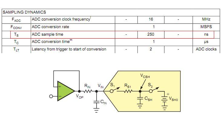
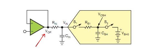
I want to set a longer sampling time so that CIN capacitor can have enough time to be stable after the sampling process of ADC of TM4C123GH6PGET. But I dont know how to set this in datasheet. I see in datasheet that ADC sample time is 250ns, so we can change this time. Anybody can help me. Thanks.

  • As you've hinted (likely suspect) that sampling time is pretty much, "off limits" to we users - achieved w/in the MCU and no (known/public) specification details how - or if - sampling time can be altered.

    Like you - we've noted some drift w/in ADC's of this nature - this MCU maker and others.  (i.e. this is not a weakness experienced alone by this vendor)  Realize that such, "mixed signal" ICs - while attempting to offer "much expanded capabilities" - often lack some of the refinement & precision of, "devices focused tightly to task."

    You can reduce ADC errors by properly mating your outside world, analog signal's impedance, to your ADC's input.  You may note - as we have - that wide voltage excursions - w/in sequential analog "steps" - tend to cause the more recent channel in the sequence to suffer apparent, "signal bleed/encroachment" from the preceding signal.  We've found that a 2nd read - of that same channel - often yields improvement.  (i.e. that placement of a repeated channel selection greatly reduces any channel to channel, signal bleed or cross-over - caused by a preceding channel in the step sequence.)

    You may also experiment with the conversion rate - enabling more time between conversions seems to dilute this signal bleed...

    Unstated of course is why this has grabbed your focus - and what your (reasonable) ADC expectations are...

  • Hello Quynh,

    On TM4C123 this has been a well noted issue due to increased source resistance and for the moment the only way to go around this is to perform multiple samples of the same channel and pick up the last reading. How many conversions to be done, depends on the how large the source resistance is. Alternatively, a Voltage follower would help.

    On TM4C129 this has been changed and the user has control over the sampling time so that a higher source resistance can be overcome without the need for additional components.

    Regards

    Amit

  • I want to measure voltage(Vop) precisely less than 3mV. So if Rin=1k OHM, Cin=1nF, Vop=3V. Affter sampling time(250ns), Cin voltage is 2.98V (deltaVop=20mV>2mV),because Cin charge to CADC. Do you know hơ to fix it?

  • This is straightforward but there are a number of picky details.  This is an issue common to all multiplexed A/Ds whether internal or external regardless of manufacturer.  TI has actually given the information needed to solve it directly which is not always the case.

    I am going to assume you actually mean accuracy rather than precision.  If you do mean precision the answers are slightly different.

    The first issue is that CSH must have a voltage that matches CIN after the sample period.  You can neglect RS1 as long as the manufacturer has set the sample period correctly and the series resistance on CIN is small compared to RS1.  If the manufacturer has not set the sample period correctly there's not much you can do.  As long as the sample period is short RIN effectively isolates the external signal from the signal so you can neglect any current in RIN.  In order for your sample voltage on CSH to match the initial voltage on CIN to within xV you must be able to completely charge or discharge CSH without changing the combined voltage by more than xV.  The worst case for this is when the two capacitors are at opposite extremes of voltage (which can easily happen if two neighbouring channels are at opposite extremes of voltage)  so you want CIN > VMAX*CSH/xV.  This is normally easy to do. 

    The second element to consider is your reference.  It must be accurate and stable enough to support this.   3mV/3.3V  --> a better than .09% reference.

    The third element that must be satisfied is the accuracy of the A/D converter itself.  Check the data sheet.

    The fourth element is the gain and offset errors on your sensor input must be accurate enough and the impedance low enough that you can keep CIN accuractly charged over the frequency range of interest.

    Finally note that it is the sum of these errors that provides your final accuracy so if any one of them just meets your accuracy result than any error in any of the others will mean your final accuracy does not meet your needs.


    Robert

    A side note.  Effectively the sampling circuit imposes much higher frequency requirements on yout input circuit than your sampling rate does.  Sometimes by several orders of magnitude or more.

  • A note on A/D accuracy. 

    You are asking for 3mV in 3.3V  That works out to about 3LSB (least significant bits).  The data sheet on the micro I am using states the Total unadjusted Error max and +/-30LSB so you are starting off asking for something beyond the capabilities of the micro unless yours had a better A/D subsystem. 

    This error specification is based on a number of assumptions and you can certainly break some of them and improve on matters but it is a non-trivial task.

    Robert

  • @ Robert,

    Keen and well-focused detail - helpful to many - thank you.

    Indeed - horse bound for glue-factory - unlikely to be high-finisher - May's Kentucky Derby.  Thus the proper "mating of device to task" - as my opening post argued, "Realize that such, "mixed signal" ICs - while attempting to offer "much expanded capabilities" - often lack some of the refinement & precision of, "devices focused tightly to task."

    Thorough read/review of the device spec often reveals, "suitability for purpose" - and as your analysis clearly shows -too often is neglected...  (i.e. all the input "massaging" in the world will not save this poster...)

  • That is SYSTEM PERFORMANCE when using internal reference. SYSTEM PERFORMANCE when using external referencen is +/- 4LSB. But I can calib offset and gain error.

    The first issue, you said that CIN > VMAX*CSH/xV. But I need a time about t=9*CIN*RIN(ADC 12bit) to charge fully CIN before sampling process. That is too long.

  • Quynh Dao Van said:

    That is SYSTEM PERFORMANCE when using internal reference. SYSTEM PERFORMANCE when using external referencen is +/- 4LSB. But I can calib offset and gain error.

    Definitely an improvement but still larger than your stated requirement even before other errors such as your reference.  Also isn't the 4lsb just the non linearity?  You don't easily calibrate that out.  Gain and offset you can with several good stable calibration sources provided you have a good stable reference.

    Quynh Dao Van said:
    The first issue, you said that CIN > VMAX*CSH/xV. But I need a time about t=9*CIN*RIN(ADC 12bit) to charge fully CIN before sampling process. That is too long.

    Amit noted that the resistance was larger as well.  Do you have a reference for how much?  Certainly the data sheet values suggest a short enough time constant.  If this is true than you are out of luck.  As I noted, if the manufacturer doesn't provide a long enough sample time you really don't have any options. Your only way of approaching your requirements is to give up the multi-channel nature of the input.  Depending on the internals even that might be iffy.

    Robert