This thread has been locked.

If you have a related question, please click the "Ask a related question" button in the top right corner. The newly created question will be automatically linked to this question.

ADC channels affected by other channels

Other Parts Discussed in Thread: TM4C123GH6PM, TM4C1294NCPDT, LM324

Device: TM4C123GH6PM

I have an ADC measuring my li-ion 3.7V battery voltage (through a voltage divider, two 180k resistors.) I also have a light sensor on my board (simple non-RoHS CdS cell due to having a few left over.)

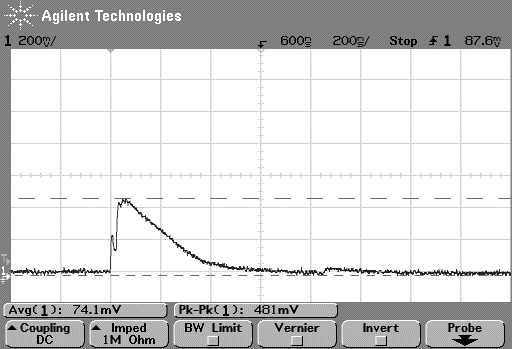
This works, but when the light sensor intensity (resistance) changes, and hence voltage on the AIN0 channel changes, the reading on the AIN2 channel is affected. A full scale range from 0~3.3V on AIN0 affects AIN2 by about 20%. Note I'm not even sampling the channel in question. Only sampling channels AIN2 and AIN3. I haven't checked if it works the other way around or on other channels.

At all times, my analog inputs are within operational limits (0~3.3V.)  VDDA is powered from 3.3V and GNDA is connected - though no particular precaution has been taken in ensuring the grounds are separated or analog 3.3V is isolated from the digital 3.3V, I would only anticipate a noise floor increase....

I'm enclosing my code. I check readings of each channel alternately. I don't require oversampling or high performance - I only check each input about 10 times a second.

I'm unsure if this is a PCB/layout problem, a misunderstanding of device capability, or a software problem, or some combination of all three.

/*
 * Initialise and start the ADC.
 */
void init_adc()
{
	// Start ADC peripheral clock and start GPIOE (if not already started) 
	// for PE0, PE1, PE2 and PE3, the analog GPIOs.
  SysCtlPeripheralEnable(SYSCTL_PERIPH_ADC0);
	SysCtlPeripheralEnable(SYSCTL_PERIPH_GPIOE);
	// Set analog mode on the appropriate pins.
	GPIOPinTypeADC(GPIO_PORTE_BASE, GPIO_PIN_0);
	GPIOPinTypeADC(GPIO_PORTE_BASE, GPIO_PIN_1);
	GPIOPinTypeADC(GPIO_PORTE_BASE, GPIO_PIN_2);
	GPIOPinTypeADC(GPIO_PORTE_BASE, GPIO_PIN_3);
	// Use sequence 3 type sampling. According to the ADC module datasheet, and
	// some example code, this will sample on the processor's signal.
	ADCSequenceConfigure(ADC0_BASE, 3, ADC_TRIGGER_PROCESSOR, 0);
	ADCReferenceSet(ADC0_BASE, ADC_REF_INT);
	ADCIntEnable(ADC0_BASE, 3);
}


/*
 * Get a sample on an ADC port (AIN0~AIN3). 12-bit result returned.
 */
unsigned int adc_get_sample(int ain)
{
	uint32_t sample[1];
	uint32_t adcins[] = {ADC_CTL_CH0, ADC_CTL_CH1, ADC_CTL_CH2, ADC_CTL_CH3};
	// Wait for ADC to be free.
	// Configure and start the sequence of conversions - containing a single conversion.
	ADCSequenceDisable(ADC0_BASE, 3);   
	ADCSequenceConfigure(ADC0_BASE, 3, ADC_TRIGGER_PROCESSOR, 0);    
	ADCSequenceStepConfigure(ADC0_BASE, 3, 0, ADC_CTL_IE | ADC_CTL_END | adcins[ain]);
	ADCSequenceEnable(ADC0_BASE, 3);
	ADCIntClear(ADC0_BASE, 3);
	ADCProcessorTrigger(ADC0_BASE, 3);
	// Wait for the result to be acquired, then return it.
	while(!ADCIntStatus(ADC0_BASE, 3, false)) ;
	ADCIntClear(ADC0_BASE, 3);
	ADCSequenceDataGet(ADC0_BASE, 3, sample);
	return (unsigned int)sample[0];
}

/*
 * Get an averaged (128x) ADC sample.
 * TODO: use ADC pipelining to improve speed.
 */
unsigned int adc_get_sample_avg(int ain)
{
	int numsamp = 128, sampctr = 0;
	unsigned int acq = 0;
	while(sampctr < numsamp) {
		acq += adc_get_sample(ain);
		sampctr++;
	}
	return acq / numsamp;
}

/*
 * Get current temperature in degrees C, using the board
 * temperature sensor. Used for speed of sound compensation.
 *
 * Note: this does not read the TIVA's temperature sensor.
 */
int adc_read_temperature()
{
	return (adc_get_sample(3) * CALFAC_ADC3_TEMP_SNS_SCALE) + CALFAC_ADC3_TEMP_SNS_OFFSET;
}

/**
 * Return in millivolts current battery voltage. 
 */
unsigned int adc_read_vbat()
{
	return (adc_get_sample_avg(2) * CALFAC_ADC0_VBAT_SCALE) + CALFAC_ADC0_VBAT_OFFSET;
}

Any advice appreciated.

  • Suspect that your 180K divide R renders the ADC input vulnerable to your noted effect.  Might you impose an op amp - config'ed as voltage follower - between that divider & ADC input?  (such will lower the signal impedance felt @ that ADC input - we've employed that method w/success - and serves as a protection element for the MCU as well)

    You may also insert a series R - best matching the input specification of your MCU's ADC input.  (rear of data manual - ADC Section - should specify)

  • Hello All,

    the scenario mentioned here seems to be inline with the errata on ADC "A Glitch can Occur on pin PE3 When Using any ADC Analog Input Channel to Sample". This in conjunction with the very high inout resistance on the other channels, can cause the readings to show deviations.

    One way is to not use channel AIN00 for the Light Sensor and instead use another channel with AIN00 remaining in digital mode and not as ADC Pin.

    Regards

    Amit

  • Hmm, is there any way to work around this? I can't readily revise the board :(. 2nd rev has already been submitted for manufacture before this bug was found.

    I'll read that errata. I do recall seeing spiking on AIN0 when scoping it.

  • Looks like you hit the nail on the head. Here's the VBAT ADC input (AIN2)

    There's clearly a sag of about 150mV, which varies with the LDR's light level, though interestingly it seems to be only worse if it's very dark; increasing light (dropping resistance) doesn't affect it.

    I'm wondering if a capacitor on the VBAT point could help improve this, by offering the ADC a nice low impedance source to sample from? Alternatively, can I lengthen the sample-and-hold period? Maybe by downclocking the ADC from the normal sample rate of about 1MS/s...?

     ?

  • Hello Tom,

    A low impedance would help. On TM4C123x series the sample and hold period is fixed and downclocking will not help.

    Regards

    Amit

  • I'll try adding a 100n capacitor across the lower resistor.

    Out of interest, what would be the accepted method for trying to measure a li-ion battery voltage? Say my project needed to go into hibernation - ~5uA - but wake up on low battery. My ADC divider alone (with ~1k resistors) would suck about 1.5mA of quiescent current. The only solution I could come up with would be an NFET in the lower resistor, or using a GPIO pin to connect the lower resistor to ground, but it seems somewhat awkward and overcomplicated, possibly introducing errors due to the finite saturation voltage of the IO or NFET.

  • Hello Tom,

    Adding a low level cap would help. Another alternative would be re-wire the channels if it can be done by trace cut after PCB is done but before assembly.

    It is a little tricky here. If you decrease the R then the battery in quiscent state consumes more current, but if you increase R then current charge capacity for the ADC becomes poor. Ideally I would prefer to have a OP-AMP to ensure that the current is not sunk majorly from the battery, yet at the output it drives the ADC Cap.

    Regards

    Amit

  • Amit Ashara said:
    I would prefer to have a OP-AMP to ensure that the current is not sunk majorly from the battery,

    One notes the initial response outlined such Op-Amp usage - which provides "twin benefits" of providing lower impedance drive to the ADC while enabling lower current flow thru a (higher R) divider network.  (follow on posts now gravitate toward the "far earlier" posting - thus are substantially derivative...)

  • Just an update: adding that cap makes a HUGE difference. No light sense issues! ADC line input has none of that awful sinking on it. The ADC is also a lot more accurate - before I had to have a significant scale factor deviation from the expected 6.6V for full scale 4096 code, now it is dead on 6.6V with just a 10mV offset, probably attributable to the resistor divider current into the ADC and 1% resistors.

    If you've got a low power need and low frequency sampling (in my case about 50Hz) then you should be able to use high value resistors IF you put that cap in place to give the ADC a nice low impedance source to sample from. I'm guessing the cap size would be determined by the ADC's sample-and-hold capacitance and the required error, for me, a 100n cap worked because I have a strip of them left over, with 180k divider resistors this puts the 5RC point around 90ms, which is fine for me. Battery voltage won't change fast enough for that to be a problem.

  • I have a similar problem with TM4C1294NCPDT.

    I use only two A/D channels AN18 and AN19, which are connected to two potentiometers through op-amps used as buffers.

    When both of potentiometers are at minimum, the channels show 0. When the voltage at AN18 is rising close to maximum (3.3V), at some point AN19 starts to show non zero values (I only use upper 8 bits of the conversion, so the error is pretty big) .

    After reading this post I've measured again the voltage at AN19, and this is what I see every time AN18 approaching 3.3V:

    This spike rises gradually. The higher the voltage at AN18, the higher the spike at AN19.

    Another thing I noticed:

    When I change the order of conversion (AN19 first, AN18 second), the phenomena "moves" to AN18 (rising at AN19 affects AN18).

    It seems that somehow the second conversion is affected by the first.

    Any ideas how to solve this issue?

    Thanks.

  • Can it be that the internal sampling capacitor is not discharged (or doesn't discharge fast enough) between conversions?
    I changed the value of S&H Width to maximum, but there was no effect.
  • Hello Michael

    My initial thought was the same as the S/H capacitor. But the timing change will help with the sampling time for the value and not the charge couple from one channel to another. Is this the case on AIN18 and AIN19 or are other IO's (may be a unused IO) shows the same behavior?

    Regards,
    Amit
  • For quick/easy test you may employ the "8 step sequence" w/the channels of interest greatly separated.  (w/in that sequence) 

    In theory - if the S/H cap is the culprit - the "bleed" effect will "amplify" as those channels come closer w/in your step sequence...

  • I changed ADC frequency to minimum (with PLL) by using

    ADCClockConfigSet(ADC0_BASE, ADC_CLOCK_SRC_PLL|ADC_CLOCK_RATE_FULL, 63);

    because my working freq is 120 MHz, this changes ADC freq to around 7.5 MHz. Didn't help.

    Then I lengthen the S&H window to maximum

    HWREG(ADC0_BASE+ADC_O_SSTSH0) = 0x0c;

    Didn't help.

    Finally I decided to use 2 different sample sequencers, one for each input. This solved the problem for me (along with the two previous modifications). The spike is still there (and I still believe that it's the internal s&h capacitor), but I guess because of the different timing of sequencers, the samples are not affected.

  • Hello Michael,

    You are correct, the spike will be there based on what the two channels are charged to. Timing would not be affected by use in different sample sequencers unless the sampled channels are separated in the sequencing.

    Regards
    Amit
  • Isn't the internal S&H capacitor supposed to be discharged before switching to the next channel in the sequence? Because every time the first channel will have higher voltage than the second, it will affect the second conversion in the sequence (and it's exactly what happened to me).
  • Isn't the internal S&H capacitor supposed to be discharged before switching to the next channel in the sequence?

    No, it is not. This is supposed happen across the effective input resistance of your ADC, that in turn happens to be an 'intrinsic' resistor of the ADC and the output impedance of your driving circuitry. That's why ADCs usually specify a maximal resistance - otherwise the S&H can not fully charge/discharge in the next sample phase. Between sampling phases, the capacitor is disconnected, and only some leakage occurs.

    In short, I think you need to redesign your input circuitry. Either use lower values for the voltage dividers, or use a buffer amplifier. The S&H capacitor and the input resistor(s) form a simple RC element, which can be used for a rough calculation of the timing.

  • Both of my channels are connected directly to op-amps used as buffers. The voltage can change between 0-3.3V, and the bigger the difference between channels the larger the error of 2nd channel conversion.
  • Op-amps could (but not necessarily do) have low output impedance. A series resistor would destroy the effect. The "sample phase" of an SAR-ADC means effectively, that you need to charge the S&H capacitor across the input impedance during the sample time. Hence my suggestion to do a rough calculation with an RC element, representing the impedance/S&H-cap combination.

    Did you estimate the effective input impedance of your circuitry, and compare it to the value given in the datasheet ?

    As a simple test, you can connect low-resistance voltage dividers (1k .. 5k) directly to the AIN pins. A cross-over effect should not be present then. (I might read the TM4C datasheet again to check for the actual numbers ...)

  • Greetings f.m.,

    Always glad to see your arrival (both here & other ARM fora).

    Now - I'm in general agreement with your writing - yet my small firm has noted the near identical effects as poster reports - and we too employed op-amps as buffer elements.   (fronting the ADC)

    May I note that there may be variances in the output impedance of different grade/type op-amps?   And - even if the op amp IS imposed between higher impedance signal and the MCU's ADC input - if the op-amp is not outputting (near) 0V - it may not be able to fully/properly "discharge" the ADC's S/H cap.

    Perhaps a better "strategy" is to briefly drive the ADC input to ground -for a sufficient time - and (only then) attempt the desired "next" conversion.   (that brief channel discharge signal is - of course - removed prior to the "next" conversion.

    Let the record show that we've noted this "channel bleed" across ARM MCUs from multiple vendors (my firm uses 5 different vendors).

    What I've presented here is "theory" we've not yet test/verified - perhaps one here can, "try & report..."

  • As an amplifying "follow up" to my post (above) we note such, "Sequential Channel Signal Bleed" when the channel "Voltage Levels" are reversed - as well!  (e.g. assume the 1st channel in the sequence is at/about 0V5 - the 2nd channel at/about 2V5 - that 2V5 reading will be "reduced" - apparently "impacted" by the preceding channel conversion!)

    When an extremely critical measurement "must" be achieved - it appears that one must apply an "artificial" channel level - as close as possible to the, "critical channel measure" as possible - both in voltage level and channel's step sequence.

    Another method my firm has developed is to devote the FULL, 8 channel step sequence - to the measurement of a single, critical channel!   This of course slows/retards the conversion process - yet "escapes" the effects of signal bleed upon the S/H capacitor.

    Again - most all ARM MCUs we've tested (multiple vendors) exhibit this signal bleed.

    As a result - when serious/critical measures are required - my firm's preference is a, "stand alone ADC" located far from noise & switching digital signals (even shielded - a la scope input techniques) when required.

  • There is not only the output impedance of the op-amp to consider but also its ability to drive a capacitive load and its response time. In order to feed a sampling circuit like the one in the TIVA the op-amp needs a bandwidth on the order of 10's or 100's of MHz.

    There is a lot to be said for a simple R/C filter just before the A/D input. The large C will not be affected by the S/H voltage and the impedance will be low, greatly reducing the sampling bleed (essentially to zero). It's also stable and it reduces the bandwidth of any op-amp required (now you only need to match the R/C bandwidth).

    Robert

  • @ Robert,

    That's a good point - yet we've tried (both) "jelly bean" LM324 as well as another's AD8251 (10MHz Instrumentation Amp) and noted only minimal "escape" from this signal bleed.  As the need for rapid conversions increases (as it always/ever does) the R/C filter suggestion declines in value & utility...

    Under the identical "front end" (In Amp or Op Amp) - the "real, stand-alone ADC" does not suffer this bleed effect!

    MCU as "kitchen sink" (i.e. Do everything) may be good on paper - Not so much (in the real world!)

  • Hi cb1,

    you are correct -  "rail-to-rail" becomes a serious issue with such low voltages. Where cost do not matter too much, I supply opamps from +5V (USB), and -5V generated by a 7660 voltage converter circuit.

    Not sure if your "drive to ground briefly" method does not mask the issue. Instead of a "drag" from the other channel, I would expect a "drag" from ground, i.e. the conversion value actually be too low.

    I have seen other post about "channel bleed" for other MCUs, but that mostly turned out to be an inproper configuration (sample time too short for input resistance / S&H cap combination). This gets really tricky for high speed conversions, as for motor control applications. I like the part of another vendor, which has 2 or 3 ADC which could be synchronized for such applications ...

    But as you stated earlier in this thread, a MCU, as a mixed-signal IC, is always a tradeoff. The ADC section is surely far from being perfect, and this "channel bleed" might be an intrinsic problem (for instance caused by a parasitary series resistance to the S&H cap), dunno. Never had such issues with my (competitor's) MCU ...

    In that case, one could either space conversion of channels further apart in time, increase the sample time, or try a cheap external ADC.

  • Hello Robert

    While the op amp bandwidth is critical I do not think it is in the order of 100's of MHz.

    Regards
    Amit
  • Hi f.m.,

    Indeed - just as you state - signal "drag" occurs (near equally) when V_ CHn > V_CHn+1 (in step sequence) or V_CHn < V_CHn+1.

    Our "method" (devote 8 - or just 4) successive step sequences to the conversion of a SINGLE Channel - underlines the futility of "kitchen sink" MCU expansion... "Real ADCs" exist for a reason...
  • Amit, rough back of the envelope testing breeze with a wet finger.

    Sampling period is often around 10% of total conversion time. With 1MHz conversions that give you 0.1uS to charge the sample capacitor. Basically you have a 10MHz square wave which requires 100's of MHz of bandwidth to form.

    You don't need to get quite a square wave charge but you do need to get the final result to match to a small fraction of the total so 100's of MHz bandwidth is not an unreasonable estimation.

    Robert
  • The R/C simply bridges the gap between sample time and conversion period. At high speed it's only a 100:1 difference or so, at lower conversion rates the frequency discrepancy gets much larger given a fixed sample period.

    As you say a non-muxed ADC is easier to deal with in this regard. Similarly a muxed A/D on a fixed channel. In that case your frequency requirements are considerably lower.

    Robert
  • I think I need to admit that I did not use the TM4C ADC yet. So, when I actually read the regarding section of the datasheet, I was really surprised. There seems to be no option to set the sampling period !

    The (competitor's) device I mostly use allows for 8 different sample period settings between 1.5 and 600 ADC clock cycles. Assuming the Tiva ADC has the same features seems a little bit ignorant on my side ...

  • f. m. said:
    Assuming... ADC has the same features... seems a little bit ignorant on my side ...

    I much doubt that mon ami.   Yet proper "investigation" (properly comparing/contrasting) the array of features - across multiple ARM MCU vendors - appears a "far greater" ignorance!   (clearly avoided by you)    And (sadly) one (too often) in practice - this forum (especially) and others.

    At the "savings" of a, "Not quite ready for prime time IDE" (my opinion: SWD - long a standard - has (yet) to make an appearance) users (knowingly) "Lock themselves into ONE Vendor - forever!"   (wise that - or not!)

    Vendors (constantly) (mostly) "leapfrog one another" - believing one vendor to "always/forever" be "top dog" may not pass "sanity test."   (but the underperforming, strictly limited IDE - was "free")   I go in peace...

  • Unfamiliarity breeds complacency? ;)

    FWIW, in my experience programmable sample times are a minority. I've also never really seen the point of them, generally the only use is to degrade accuracy for a small increase in speed but there are no doubt uses (or at least people who believe they have uses) for it.

    Robert

    Although at 600 A/D cycles I'm left wondering if they aren't compensating for a high impedance S/H setup.
  • FWIW, in my experience programmable sample times are a minority. I've also never really seen the point of them, generally the only use is to degrade accuracy for a small increase in speed but there are no doubt uses (or at least people who believe they have uses) for it.

    All STM32 parts have progammable sample times. BTW, 600 is the upper limit (it's actually about 600 but not exactly).

    And concerning "not seeing the point of them", the mere existance of this thread should be a point.

    I see no point in enforcing a sample time of 250ns for ADC sample rates of a few Hz or mHz ...

  • f. m. said:
    FWIW, in my experience programmable sample times are a minority. I've also never really seen the point of them, generally the only use is to degrade accuracy for a small increase in speed but there are no doubt uses (or at least people who believe they have uses) for it.

    All STM32 parts have progammable sample times.

    Even with that added it would still amount to a minority of the A/Ds I've worked with2.

    f. m. said:
    I see no point in enforcing a sample time of 250ns for ADC sample rates of a few Hz or mHz ...

    Allowing it to change makes no difference to your implementation1. You need a low pass filter and having that filter contain a capacitor in the final element adds no cost and eliminates any issue from the shorter sample period.

    Sigma-Delta is another kettle of fish

    Robert

    1 - Other than making the control SW more complex.

    2 - There were, maybe still are, A/Ds without a built-in S/H.  In that case external S/H or T/H circuits were necessary. Sometimes they had the capability to adjust sample period for a speed of acquisition/accuracy trade-off.

  • See also

    www.ti.com/.../slyp166.pdf

    A nice set of graphs (Pgs 31-36) showing load transients from sampling. Note that the figure on pg 33 showing that simply reducing the signal impedance is insufficient to reduce the spikes w/o the capacitor (although the width does look narrower).


    Robert
  • Robert,

    Quite a terrific document Robert - outstanding of you to share it - thank you - we are in your debt.

    That said - placed in this non-descript thread - it will (shortly) rotate off home page into forum oblivion.

    May I suggest (well deserved) better fate?   Create a new post - properly highlighting this ADC centric wonder.   (may prove easier to search/find)

  • I've considered doing a care and feeding of A/Ds post including this and the earlier reference. Maybe in my copious spare time, surely to be followed by my grand unified theory. :)

    Robert
  • Allowing it to change makes no difference to your implementation1.

    I beg to disagree.

    The sampling time is basically the time you have to charge/discharge the S&H capacitor to the voltage level of the input channel. The shorter the time, the higher the current needs to be, i.e. the higher the requirements for the driving circuitry regarding output impedance and bandwith. If the time is too short (or the impedance/bandwith parameters are insufficient), you get this kind of "cross channel leakage".

    ST might have designed their ADC peripheral with other applications than motor control in mind ...

  • Dislike the sense of, "Disagreement" here - posters f.m. & Robert have both - provided significant "enlightenment" (credit poster Luis) into the "inner workings" of the MCU's SAR ADC.

    My small firm has steered hard starboard - never "buying into" the MCU as, "Do all - be all."   (i.e. kitchen sink)   And - in each/every "serious" product "teardown" or review we've seen - never was an MCU chosen to perform critical, ADC measure.

    The desire to "reduce costs" by employing an (admittedly) compromised ADC - I believe - is mistaken.   Far and away - those here - should not be striving for such minimal cost savings.   Instead - profit margins should enable the search for, identification of, and selection of the best, properly focused components - to fully meet the product's objectives.   In addition - specific to this, "Care/feeding of an ADC" - is the "on-going" variation in hardware & software - imposed by even the same vendor - let alone the multitude.  (e.g. when moving between different MCUs)  

    Selection of a "real/dedicated" ADC IC (instead) enables its quick/eased/high-confidence "reuse" across multiple applications.   And - the discrete ADC may be placed "exactly where it makes the most sense" (far from digital and/or power switching & other "noise") and even "entombed!" (electrically - even magnetically shielded - as noted in serious scopes & pro data converters.)

    Searching for - finding a niche market - and then "outperforming the competition" enabled my past tech firm to grow from zero to 17M (USD) w/in 4 years - and go, Public...   Suggested (above) is just one of the methods which, "drove to that objective..."

  • Heh, not referring to motor control actually.

    Let me see if I can explain why I don't see extending the sample time as useful most, if not all of the time.

    You will have a filter on your analog signal. With a10pf sample capacitor if your capacitor adjacent to the A/D pin is 0.01u then you have a setup where the sample capacitor voltage differs from the input by less than 1 part in 1000, getting close to the practical limit of the device. By increasing to 0.1u you get to a point much better than the A/D is capable of. These are still well within fairly standard C0G/NP0 ceramics. Of course, if you are after 16 bit accuracy you need to do more work.

    If you choose your capacitor in that fashion you can choose an accompanying resistance to ensure that the capacitor is restored before the next sampling point.

    You can reduce the capacitance but in that case you impose additional requirements on the rest of your signal conditioning to provide charge to the sampling capacitor

    Robert
  • Heh, not referring to motor control actually.

    To me, it just seems TI is mostly targeting motor control and similiar applications. Things like short sampling times, multiple options to synchronize sampling with other events (i.e. triggering), and multiple, synchronizeable channels suggest so.

    ... These are still well within fairly standard C0G/NP0 ceramics. Of course, if you are after 16 bit accuracy you need to do more work.

    While I'm basically with you, I would not seriously try a 16 bit ADC integrated in a "noisy" MCU, and rather go for an external solution.

    If you choose your capacitor in that fashion you can choose an accompanying resistance to ensure that the capacitor is restored before the next sampling point.

    That applies if you have a low-impedance source, or a buffer amplifier.  There is a multitude of very-low bandwith sensors that could connect directly to the ADC input - if the sampling time is significantly longer than 250ns. That allows for less parts and cheaper solution. If any form of "software correction" (like averaging in this case) is possible, project managements often choose this cheap route. I have experienced this often, albeit mostly for projects involving 8/16 bit MCUs, or Cortex M0 devices.

    Generally, I agree with cb1 in this regard. PMs and R&D departments often show very little loyality to a "brand" if it doesn't fit the current needs. And on the vendor's side, this has the positive effect of avoiding complacency and stagnation in the long run ...