This thread has been locked.

If you have a related question, please click the "Ask a related question" button in the top right corner. The newly created question will be automatically linked to this question.

I think TI's Crystal cap. calcs for the TM4C129X are in error

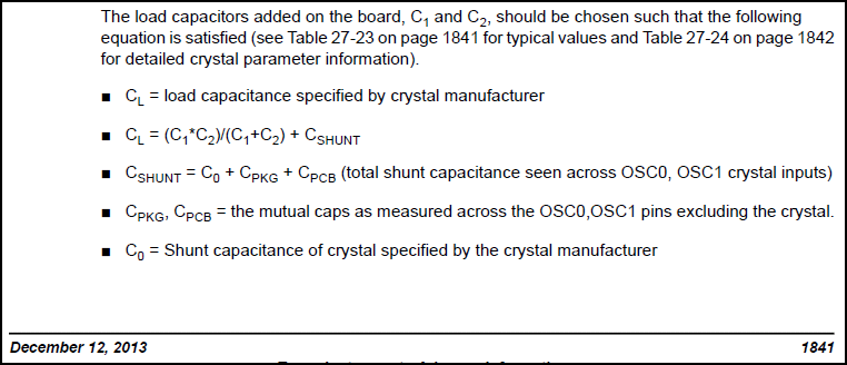
This discussion has part academic value and part practical value.   I believe TI have made an error in their formula for CL, the load capacitance specified by the crystal manufacturer.   TI went to great lengths to list specific crystals from a variety of manufacturers for which TI provide calculated values of C(=C2 ).

To summarize, I have found NO Crystal manufacturer which requires you to use C0 (the crystal's shunt capacitance) when calculating C1,C2 from CL or visa versa.    You can search for yourself  for formulas online, and I am happy to copy excerpts from Statek and Abracon in emails they sent me stating this fact.    However see below for the formula given by TI as cut from p. 1841 of their datasheet which includes C0.

As long as your chosen crystal's Cis low enough (e.g. 1-2pF) then in practice the values calculated for C1=C2  are sufficiently similar to those obtained when excluding Cfrom the formula.  If Cis higher (e.g. I am using a crystal with C0=7pF) then the values calculated for C1=C2 are nearly half  (18pF c.f. 32pF for a given CL of 18pF) !   For some entries in table 27-24,  C0=3pF and the resultant values for C1=C2 are too low by about 6pf (i.e. 18pF c.f. 12pF).   This could be significant.

Because I want my oscillator to start up first time for the life of my product under all temperature and component tolerances, I wanted to ensure I had a good handle on this aspect of the design so this mistake in TI's formula has lead me to spend a LOT of time trying to make sense of it because I had put implicit trust in TI and initially didn't assume they were wrong.  One product recently in development in my company failed to reliably start oscillating and  either due to lack of knowledge or misinformation the electrical engineers gave up and opted to drive the OSC pins with an oscillator module instead !  That shows how important it is to ensure the formulas are correct.

Unless your crystal's C0 is >2pF then, you will probably never notice this error nor care about this discussion !

  • Peter John said:
    Because I want my oscillator to start up first time for the life of my product under all temperature and component tolerances, I wanted to ensure I had a good handle on this aspect of the design so this mistake in TI's formula has lead me to spend a LOT of time trying to make sense of it because I had put implicit trust in TI and initially didn't assume they

     Hi Peter, formulae are correct and calculate equivalent capacitance of load cap to resonator, CL are the load cap, resonator see them in parallel to so they where in series from formula. Again capacitance of all pcb track and crystal case are in parallel to. Get recommended value from manufacturer then choose loading capacitor.

    From table I see more questionable series resistors in the range of KOhm, at these frequencies they can filter out oscillator.

     On all design I finished these day I inserted both crystal and oscillator pinout, I got impressed by this part from mouser :634-501JCA25M0000CAG price is comparable to resonator and pinout can serve both configuration.

  • Roberto Romano said:
    Hi Peter, formulae are correct .  

    Hi Roberto, thanks for your reply.  If you believe the formulae are correct, are you able to prove this by showing me at least ONE crystal manufacturer that publishes a formula which includes C?  On the contrary, each manufacturer I have looked up (at least 5-6 ) DO NOT include C0   in the formula they give you which means they take it into account themselves when you tell them what CL you need.    In fact Statek and Abracon replied to me and explicitly said Cis NOT in the formula they give us.

  •  Hi Peter. please can you post source where I can valuate some formulae from manufacturers? I can figure a misunderstanding can come from Co max shunt capacitance to xtal termination and Cshunt that come from TI formula, this is capacintance from manufacturer (not Co max), stray from pcb and all other are on track and substrate.

     IAgain this is my point of interpreting formulae so C0 is   real shunt but not Co max.

  • Hi Roberto,

    Thanks for taking an interest.  The following manufacturers confirmed for me via email that the crystal's C0 shunt capacitance is not used in their formulas for calculating the CL load capacitance.

    Here is the formula from Statek http://www.statek.com/products/pdf/CX2SM_10135_RevC.pdf

    Here is the formula from Abracon  http://www.abracon.com/Support/facn_abracon_jul2011.pdf

    Abracon's analysis concurs with Statek's excellent technical note, they write (on p. 3).  

    There are at least three stray capacitances that must be considered in trying to calculate the load capacitance of the Pierce oscillator circuit

    1. An added capacitance from the input of the amplifier to ground.
    2. An added capacitance from the output of the amplifier to ground.
    3. A stray capacitance Cs shunting the crystal as shown in Figure 2

    Once again note how C0 is not included at all.  Cs nominated by Statek is the same as Abracon's "board strays".

    As I mentioned above if you can find even ONE manufacturer who includes C0 in their formula then I will be very impressed, but the following Google search has at least the first few hits not mentioning C0 at all !

  •  Hi Peter, there where two view point,

     from xtal pin and from osc pin,

      Co on xtal is the parallel Co of all case crystal and pin and is the one are you mentioning here.

     On TI point of view I still read "Total shunt Capacitance seen across osc0 osc1 crystal input", this mean from IC side and from IC side that formula is ok, so the series of two parallel PI resonator load, stray capacitance and even Co of resonator too is in parallel of the two oscillator pin.

     Both are shunt capacitance and both affect oscillation stability, Cshunt on oscillator pin feed ac signal to input giving a phase shift that reduce gain with frequency increase stopping crystal from oscillating, on crystal side can shift frequency and if too heavy stop oscillating again masking inductive behavioural of parallel resonating.

     I point again the only error I noticed is on resistors values on table, that resistor is for Pierce oscillator Rf bias exactly as for crystal manufacturer not Ra power limiting, more attention has to be posed on limiting resistor that can stop oscillating or wear resonator in a short time.

  • Hi Roberto,  

    If TIs definitions and formula are correct why does it give us a totally  different result for CL, (the load capacitance specified by the crystal manufacturer) when compared to EVERY other formula for Cwe can find so far ?!

    Roberto Romano said:
    On TI point of view I still read "Total shunt Capacitance seen across osc0 osc1 crystal input", this mean from IC side and from IC side that formula is ok,

    I agree their definition is from the IC side, BUT that doesn't mean it is correct to use that definition.

    Roberto Romano said:
     I point again the only error I noticed is on resistors values on table, that resistor is for Pierce oscillator Rf bias exactly as for crystal manufacturer not Ra power limiting

    The whole motivation for my post was to highlight a discrepancy between TIs value for Cand the values calculated by many other formulas from reputable crystal manufacturers .  By ignoring this error you are claiming for example that 18pF=32pF  !

  •  Peter, from data sheet:

    Parameter    Parameter Name                                             Min nominal max

    C1, C2      External load capacitance on XOSC0, XOSC1 pins  12pF           24pF

    CSHUNT  Total shunt capacitance                                                                 4pF

    CPKG Device package stray shunt capacitance
    CPCB  PCB stray shunt capacitance


    CSHUNT = CPKG + CPCB + C0 (total shunt capacitance seen across XOSC0, XOSC1)

    C1 and C2 are the values in pico Farads of the load capacitors that should be put on each leg of the crystal pins to ensure oscillation at the correct frequency. Rs is the value in kΩ of a resistor that is placed in series with the crystal between the OSC1 pin and the crystal pin. Rs dissipates some of the power so the Max Dl crystal parameter is not exceeded. Only use the recommended C1, C2, and Rs values with the associated crystal part.

    ---------------------------------------------------------------------------------------------------------------------------------------------------

     Your crystal require a 7pF load capacitor, has a parallel typical of 1pF and stray capacitances add about another pF in parallel, oscillator output is less than max so RA = 0

     Cshunt OSCILLATOR is near 2 pF from stray and crystal so it is OK with oscillator max Shunt

     Load caps need to be in the range of C1 C2, your crystal need 7 pF parallel resonance, subtract 1pF from stray and use C1= C2 series of two 12pF obtaining the correct load of 7pF.

     Resonator see a parallel Load capacintance of

    CL=(Cd*Cg/(Cd+Cg))+Cs => (12/2)+1 = 7pF as specified on data sheet.

      From where you can see 18=32???

     Again this value is low range so it can be better to select a crystal with load capacitance in the range 7.5-11.5pF...

     From this FORMULAE ARE CORRECT!!!!!

     I cannot figure where you got 32pF, value greater than 24pF or less than 12pF stop oscillation, wrong layout with greater than 4pF stop oscillator too.

     Exceeding max value at OSC pins stop oscillation, Pierce is not series resonant so wrong shunt capacitance on parallel resonant shift frequency!!!

  • Roberto Romano said:
     Your crystal require a 7pF load capacitor,

    Not correct.   7pF is my crystal's SHUNT capacitance as per my original post.   Thus your calculations that followed were in error.

    Roberto Romano said:
    From where you can see 18=32???

    Using TI's incorrect formula I calculate C1=C2=18pF as follows:

    CSHUNT = C0 + CPKG + CPCB  = (7 + 1.0 +1.0)pF = 9.0pF  (in my calcs I used slightly higher and more realistic values for CPKG , CPCB of 1.0pf rather than 0.5pF)

    furthermore

    CL = load capacitance specified by crystal manufacturer = 18pF for my crystal

    Another formula from TI datasheet:

    CL=C1*C2/(C1+C2)+CSHUNT 

    (18-9)pF = C1*C2/(C1+C2) = 9pF

    as C1=C2 , then C1=C2= 18pF

    Now compare this to every other manufacturer's formula which EXCLUDES C0

    Specifically using Statek's formula

    CL=CD*CG/(CD+CG)+CS 

    where (according to Statek) "CS is the stray shunt capacitance between the crystal terminal. CS should be minimized."  (If CS is supposed to also include the crystal's shunt capacitance (C0) as you and TI are claiming then how is the end user supposed to minimise that if they have no control over C?!?!

    CS =1.0pF +1.0pF = 2.0pF

    therefore

    18pF=CD*CG/(CD+CG) + 2.0pF , hence 16pF=CD*CG/(CD+CG)

    now as C= CG, C= CG=32.0pF

    Reprinting and highlighting the text from TI's datasheet doesn't suddenly mean it is correct information.  My claim is that the datasheet states incorrect information, namely that C0 (the crystal's shunt capacitance) should NOT be present in the formula for CL the load capacitance.

    Perhaps somebody from TI needs to step in and arbitrate or even defend their position (if possible).

  • Peter John said:
    now as C= CG, C= CG=32.0pF

     Oscillator never start,if start then frequency is far low than the one printed on case!

    Peter John said:

    Reprinting and highlighting the text from TI's datasheet doesn't suddenly mean it is correct information.  My claim is that the datasheet states incorrect information, namely that C0 (the crystal's shunt capacitance) should NOT be present in the formula for CL the load capacitance.

     Peter, I am sorry but wasting time in your wrong point of view PLEASE read the details again:

     TI point of view, if you wish a working oscillator, don't exceed max chip oscillator pin capacitance allowed:

    ACROSS OSC1 OSC2 signify what?

     Crystal manufacturer specify

     BETWEEN CRYSTAL TERMINALS!!! (Load capacitance)

    please ask a FAE from Fox, Statek and or Abracon to read this accurately and see what means Co and WHY is specified.

     You need SEE what is from OSC pin side that is DIFFERENT from crystal side.. Is elementary rule of series parallel capacitors and impedances too.

     Your calculus has two issue:

     1 exceed max value at oscillators pin so prevent pierce oscillating

     2 if oscillator in some way start frequency is not the cut of xtal, load capacintance is wrong 9pF than 7 recommended for resonance...

    http://en.wikipedia.org/wiki/Pierce_oscillator

    http://en.wikipedia.org/wiki/Crystal_oscillator

    http://www.foxonline.com/pdfs/xtaldesignnotes.pdf

    http://www.adafruit.com/blog/2012/01/24/choosing-the-right-crystal-and-caps-for-your-design/

    and many other same too...

  • Roberto Romano said:

    now as C= CG, C= CG=32.0pF

     Oscillator never start,if start then frequency is far low than the one printed on case! [/quote]

    Romano, you are correct in that it will probably not start oscillating as the max C1 is 24pF for TI's MCU, so I will opt not to use that crystal now, however it still doesn't resolve the discrepancy between TI's formulas and everyone's else's formulas.

    For point of reference here is the crystal where the shunt capacitance is up to 7.0pF

    Roberto Romano said:

     Your calculus has two issue:

     1 exceed max value at oscillators pin so prevent pierce oscillating

    I agree.

    Roberto Romano said:
     2 if oscillator in some way start frequency is not the cut of xtal, load capacintance is wrong 9pF than 7 recommended for resonance...

    I'm unsure where you get the values of 9pF or 7pF for the load capacitances, but that is secondary to my main point.

    My main point is that the equations from TI and every other mfg result in (worst case) vastly different values for C1 and C2 ?  This is more subtle when the crystal's shunt capacitance is lower (2-3pF) but nevertheless still present.

    Do you agree that TI's formula gives different  values of C1,C2 than all other manufacturers ?

  • Peter John said:

    For point of reference here is the crystal where the shunt capacitance is up to 7.0pF

     Hi, this is the family leaflet, no specific information exist, so please point me to exact model you wish use, cpu model frequency and freq stability. ON exact model I try doing calculus of caps.

    Peter John said:
    Do you agree that TI's formula gives different  values of C1,C2 than all other manufacturers ?

     Peter, please enter the processor case merge to silicon...... <When you are on processor view what you see from pin!!>

     exit processor, enter the crystal case... <Watch from case pin to outside world>...

     When you watch thru a windows, is the same when you are in house or in the garden?

     Is the same when travel a 50Ohm transmission cable  to antenna going to free space where radiation impedance at about 377Ohm or when you enter the antenna then see  the antenna cable at 50Ohm toward receiver?