This thread has been locked.

If you have a related question, please click the "Ask a related question" button in the top right corner. The newly created question will be automatically linked to this question.

TM4C1294 fvco = (Physdiv, N, MINT) or foscclk = Osysdiv

Guru 55913 points

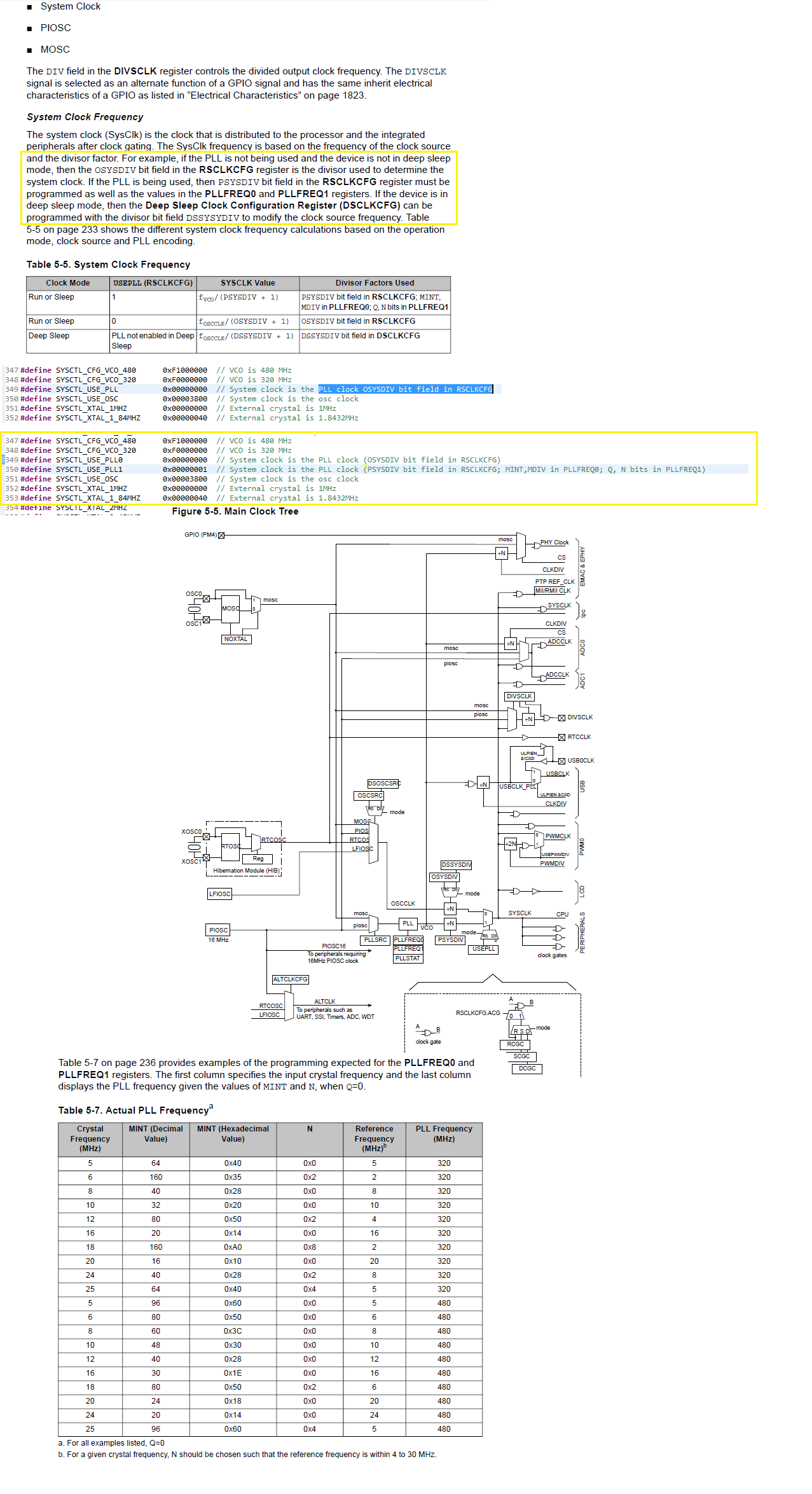
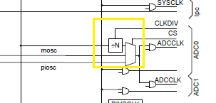
Missing clock configuration as shown in data sheet, Tiva library not keeping consistent with documented clock configuration in a clear and user friendly way. The clock tree implies clock value /N at several peripheral connection nodes yet creating such a configuration appears obscure or not possible in the most recent DL library.

 The (Sys_Ctrl_UsePll=0) defined as (Physdiv) must be set (1) in the RSCLKCFG register in order to divide 480 or 320 Mhz PLL VCO for SYSCLK.

Refering to Sysctrl.c function SysCtlClockFreqSet(uint32_t ui32Config, uint32_t ui32SysClock)

Does Sys_Ctrl_UsePll = 0 imply Physdiv or Osysdiv in this function, will adding a #Define (yellow box) work?

Table 5-7 on page 236 provides examples of the programming expected for the PLLFREQ0 and PLLFREQ1 registers. The first column specifies the input crystal frequency and the last column displays the PLL frequency given the values of MINT and N, when Q=0.


  • Hello Bret,

    SYSCTL_USE_PLL implies that PLL will be used.

    Also I checked the sysctl.h and I do not see PLL0 and PLL1 definitions (yellow box). Which version of TIVAWare are you referring to?

    Regards

    Amit

  • That's the point SYSCTL_USE_PLL should = 1  not 0 when enabling the PLL, 0 is contrary to what data sheet shows as binary value. I suggested adding both _PLL0 and _PLL1 in order to easily distinct each method used for clocking SYSCLK. There are no statements in the Tiva source text that suggests which method of clocking is configured using the RSCLKCFG register binary 0 or 1 leaving one to assume OSYDIV is configured and not SYSDIV.

    Spent couple days trying to understand how the clock tree in data sheet jives with driver library code (DL last week) in order to have ADC CLKDIV=32Mhz using PLL (/N). Desire the ADC sample rate 2Msps ends up being rough 1.8Msps @30Mhz derived from either 320 or 480 Mhz PLL when MOSC=25Mhz XTL used for Ethernet module.

    To use ALTCLKCGF clock PIOSC 16Mhz for ADC CLKDIV /2; in past Stellarisware divide by N would subtract N. Related to PCAT computer CMOS, performing a bus clock divide actually multiplies the clock source by N such that Fo=1/P and not Fo=N/Freq.

    Was there some issue in Stellarisware that Tivaware corrects behavior related to IEEE bus clock Symantec's or does the /N still actually subtract N in the ADC peripheral register when using Tivaware library?


  • Hello Brett,

    The definition of SYSCTL_USE_PLL is in the sysctl.h in driverlib.The value assigned to it is interpreted by the sysctl.c for PLL Usage. I do agree that making the define more inline with the bit value would make sense, but at this point we do not expect to change it. However it does set the USE_PLL bit which causes PSYSDIV to be taken as the divider

    ADC Sample rate of 2MSPS is derived from the PLL VCO. So for both 320 and 480MHz, the ADC Clock of 32 is feasible. How are you measuring 1.8MHz?

    Regards

    Amit

  • How are you measuring 1.8MHz?

    Mathematically using the numbers the end value for ADC analog sample rate is near 1.8Msps @30Mhz.

    Given a 25Mhz MOSC = 320,480 MHZ  PLL with PSYSDIV /N=4, MINT=64,96 the clock tree boxed /N values render 120Mhz CLKDIV unto ADC, USB, Ethernet peripheral tree nodes. Further dividing CLKDIV for example the ADC analog clock sample rate; modify the ADC peripheral register /N+1, N=4 divides 120Mhz = 30Mhz and not 32Mhz. The USB peripheral mandates using MOSC @60Mhz clock source or CLKDIV/N and SYSCLK must be at least 30Mhz. Not using USB at this time but may desire to energize this area in the near future signing the NDA.

    Question if even possible to multiply the PIOS 16Mhz clock rate upward to 32Mhz without using the PLL and maintain by way of MOSC driven PLL an 120Mhz CLKDIV, SYSCLK and use the non PLL driven ALTCLK to get 32Mhz for ADC sample clock rate?

     Running the ADC analog sample clock @30Mhz shaves 200ksps off the documented 2Msps ADC sample rate. That lower speed opens more issues with ADC Rs sample and hold window width (TSNn, NHs) values written as Tadc=1/32Mhz @2Msps. Should we use the 2Msps table values for the 1.8Msps and or is that even possible using TI provided alternate table values  for running ADC samples @1.8Msps?

  • Hello Brett,

    The ADC clock is generated from PLL VCO and not the system clock. From 320MHz VCO a divide of 10 would give the required 32MHz for ADC.

    Without the PLL a higher frequency cannot be generated from a lower frequency clock source.

    Regards

    Amit

  • The ADC clock is generated from PLL VCO and not the system clock. From 320MHz VCO a divide of 10 would give the required 32MHz for ADC.

    Perhaps you missed data sheet states two ADC clocks are required. A clock for analog block and a clock for digital block. In this case SYSCLK 120Mhz directly feeds both ADC0/1 digital blocks.  The analog block clock sources are (VCO,MOSC,PIOS) when VCO 480/N(PSYDIV) or 4 = 120Mhz.  Both ADCCLK & CLKDIV 120Mhz are further divisible in the ADC peripheral clock register /4 = 30Mhz.  Unfortunately setting the PLL VCO 320/N(PHYSDIV)=10 also makes SYSCLK 32Mhz CPU speed.

    Look closely the clock tree shows a line from the PLL VCO leading into the box /N and a line out from /N leading into the analog block as ADCCLK.

    ADC Clock Control:

    The ADC digital block is clocked (directly) by the system clock and the ADC analog block is clocked from a

    separate conversion clock (ADC clock). ((When)) The ADC clock frequency is 16 MHz and can generate a

    conversion rate of 1 Msps.

  • Hello Brett,

    1. The ADCCC Register is used to configure the clock for the Analog Block

    2. As you mentioned there are 3 sources for the Analog Block

    (a) PLL_VCO divdied by ADCCC.CLKDIV

    (b) PIOSC as the default option on ALTCLKCFG

    (c) MOSC

    When the system clock is 120MHz, the PLL_VCO Clock is 480MHz. Dividing this by 15 in the ADCCC.CLKDIV would result in the Analog Clock of 32MHz. So why would the ADC then be working at 1.8MSPS instead of 2MSPS. I can say this with confidence as this part of the logic is very well tested.

    Regards

    Amit

  • Regarding using (a) PLL_VCO divided by ADCCC.CLKDIV  Setting the PLL VCO clock assigns (N=4) (yellow Box) exists @120Mhz prior to reducing the clock rate even more in ADCCC.CLKDIV  or 120Mhz/15 = 8Mhz.

    The clock tree diagram shows (/N) already assigned the PSYDIV value of (4) PRE setting clock speed exiting  (yellow box) @120MHZ after dividing the VCO 480Mhz by (4 or N) prior to dividing it even lower at the ADCCC.CLKDIV peripheral level NOT shown in the clock tree.  Datasheet tables page 235-236 show the PSYSDIV (N) values chosen 0x4 when 25Mhz MOSOC or 120Mhz SYSCLK.

    Do you agree with that assessment or is the clock tree not correct?


  • Hello Brett,

    I checked the data sheet and if you trace the %N it comes from the PLL VCO and not from output of PSYSDIV. This %N is different from the PSSYDIV (%N).

    Regards

    Amit

  • Hi Amit,

    The clock tree from my understanding outlines the system control register however does not include the peripheral control registers. Hence me elaborating that fact with a yellow box reference. If N is not N all inclusive in the main clock tree diagram then some other letter would have been used to Offset PSYSDIV value (N) however I think that is not the case here. 

    The clock tree diagram as it is drawn infers all /N = PSYSDIV or value = (4) as programmed in the system control register; RSCLKCFG 0x400F.E000:0x0B0 Bit 9:0 R/W.

    This field specifies the system clock divisor value for the PLL. This field is used when the USEPLL bit is 1.fsyclk=fVCO/(PSYSDIV+ 1)  

    That bit field text and table page 235 header text states PSYSDIV+1, the table of N values page 236 suggest a 25Mhz MOSC (N=4) 480/320Mhz etc. 

    Should that not be the case all boxed (N) divisors need be labeled accordingly with peripheral register names or at a minimal dashed lines drawn around each peripheral node clock divisor. The clock tree diagram otherwise makes no sense to what the datasheet tables page 235 & 236 are stating the value of N to be in the main clock tree diagram on page 231 all included under the same chapter reference "Clock Control".

  • Hello Brett

    The section after the diagram elaborates which peripheral register control which clock divider in the diagram. The %N is a generic notation to imply a divider. The full description of each divider is on page 232-233

    Regards

    Amit

  • Thanks Amit,

    Do understand your point on that %N however the main clock tree diagram does not elaborate that point in a clear format therefore we have struggled to this point to make each case point very important.

    Point and agreeing with what you state as being true, the ADC analog control block divisor N (yellow box) has been drawn as a connection node leading to the ADC0/1 peripherals where the ADCCC.CLKDIV register actually exist.

    Just because the text describes ADCCC.CLKDIV register in the Clock Control chapter the main clock tree diagram appears to suggest connections to the ADC analog control block out side the scope of the main clock tree diagram. In other words the text does not correlate with how the ADC analog & digital control blocks are laid out as a module having separate registers from those of system control registers used to program the PLL divisor and SYSCLK parameters within those clocking boundaries. Simply adding dotted lines around each peripheral block in the main clock tree would clearly make (/N) exist within individual register boundaries and not appear to be a GLOBAL value (N) defined by PSYSDIV.

    Amit thanks again for making the distinction of (/N) more clearly understood.

  • This started me to believe and have a deductive conclusion (%N) was a global variable.

    The Main Clock Tree shows the Ethernet module having a (%N) divisor which can not be found in any of the Ethernet PHY, MAC or system control block registers documented in the data sheet. 

    This even more lead me to believe PHYSDIV (%N) plugged into all other (%N) locations in the main clock tree.  

  • Hello Bret,

    I agree on the Ethernet Clocking Scheme needs correction. This is already in the pipe for the next data sheet release as MOSC and PM4 are going to be the only clock Source as PLL will not meet the jitter requirements of the Ethernet Standard.

    Thanks for bringing this up...

    Regards

    Amit