This thread has been locked.

If you have a related question, please click the "Ask a related question" button in the top right corner. The newly created question will be automatically linked to this question.

SSI interface with accelerometer(H3LIS331DL)

Other Parts Discussed in Thread: TM4C123BH6PM, MSP430F135

Hi. I have trouble with Tiva(TM4C123BH6PM)'s SSI interface.

I'm using STmicro H3LIS331DL accelerometer.

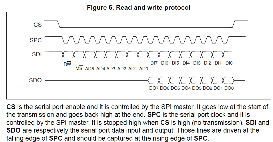
I set SSI frame format to Freescale Mode (SPH=1, SPO=1) in order to match the accelerometer's frame format.

I used the Tivaware SSI example codes. However, I changed the SSI control register to match this frame format.

-Data frame size = 16bit

-SSInClk = 2MHz (SysClk = 16MHz, CPSDVSR= 2, SCR = 3)

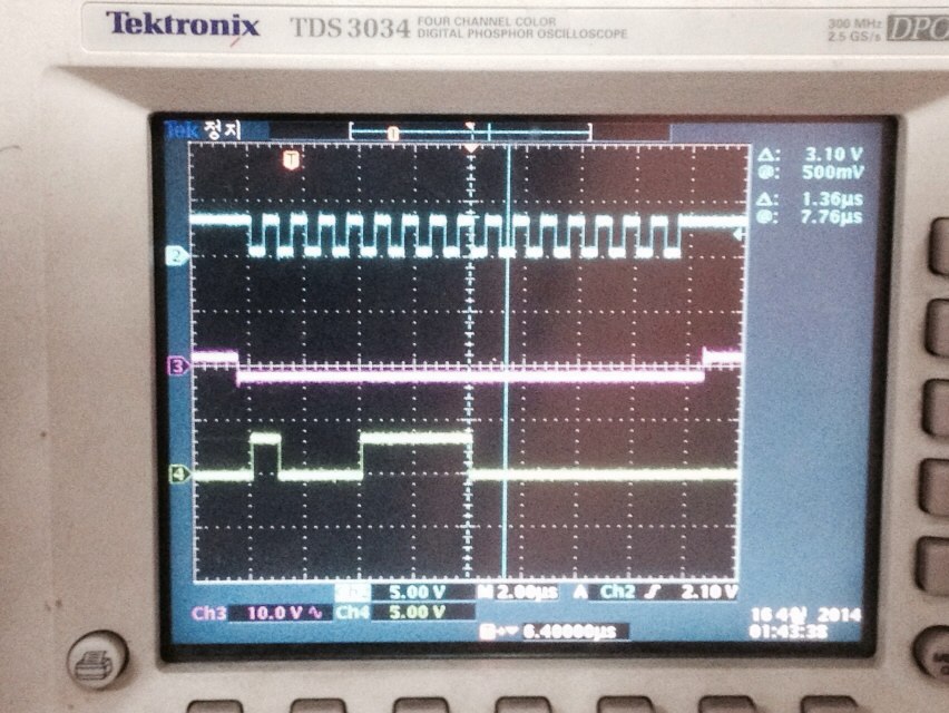
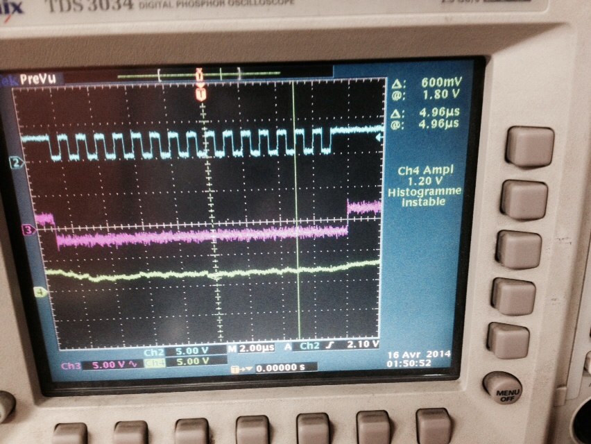
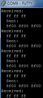
When the MCU communicates with this sensor, the RX value was only 0xFFFF

while changing the value of TX, The TX pin goes out correctly

with the wanted values(the sensor register addresses). Also the Fss and the Clock pulse was working fine.

What might be the problem?

Could it be soldering problems, difference of data order or SW problems?

  • Hello Kim,

    Do you have schematic with interfacing between TM4C and H3L devices?

    Also when the RX value is read as 0xFFFF, you may want to check the RX pin from H3L to TM4C. Does it toggle or not?

    Regards

    Amit

  • Hello Amit.

    This is the schematic with interfacing between TM4C and H3L device.

    At the oscilloscope, the RX pin(28) is keep showing 3.3V so when debugging with  CCS5,

    the value of RX was 0xFFFF. I don't know exactly whether the RX had toggle or not.

    What do you mean the RX pin has toggle?

    And how do I   configure FSS pin?


    Regards

    Kim

  • Hello Kim,

    The CS Pin on the H3 device is the selector between I2C and SPI Mode. It also functions as the Chip Select and needs to be driven 0. Since the SPI Core in TM4C can have only one CS, you need to control the same through GPIO. The GPIO has to be driven 0 for transaction.

    Regards

    Amit

  • Hello Amit.

    Does the CS pin has to be always low for the senor to select SPI mode?

    Or do I have to make CS pin low only when SSIDataPut (function in SSI.c) is called?

    In other words, do you mean that if the CS goes low, the H3 becomes SPI mode automatically?

    We made the CS pin low , but It didn't work. The Rx value was still 0xFFFF, showing 3.3V. 

    How can I do? Is it about  soldering problem?

    Regards

    Kim.

  • Hello Kim,

    Pin-2 and 3 are NC. Why have they been GND-ed?

    Also does the "WHO AM I"  register read also gives the same response?

    Regards

    Amit

  • Hello Amit,

    There was no special reason why both were GND-ed.

    However, I think there's no problem with it.

    I tried this sensor with a MSP430F135, and the sensor worked fine

    whether pin 2 and 3 were GND-ed.

    Also reading  "WHO AM I" register shows the same response.

    The value of RX was still 0xFFFF, 3.3Vs

    Regards

    Kim.

  • Hello Kim,

    Thanks, that rules out any component issue. Can you please send the code and also if possible a scope snapshot showing the CS, CLK, SDI and SDO signals for the transaction?

    Regards

    Amit

  • Hello Amit.

    My oscilloscope cannot show all 4 signals. One of the input was broken.

    Please understand the inconvenience.

    This is the signal of CLK, FSS, SDI(MCU TX).

    This is the signal of CLK, FSS, SDO(MCU RX).

    This is the signal of  SDO(MCU RX) only. It has a voltage drop.

    However, if we disconnect the sensor(taking it off using heat gun), it shows 0V.

    #include <stdbool.h>
    #include <stdint.h>
    #include "inc/hw_memmap.h"
    #include "driverlib/gpio.h"
    #include "driverlib/pin_map.h"
    #include "driverlib/ssi.h"
    #include "driverlib/sysctl.h"
    #include "driverlib/uart.h"
    #include "utils/uartstdio.h"
    
    //*****************************************************************************
    //
    //! addtogroup ssi_examples_list
    //! <h1>SPI Master (spi_master)</h1>
    //!
    //! This example shows how to configure the SSI0 as SPI Master.  The code will
    //! send three characters on the master Tx then polls the receive FIFO until
    //! 3 characters are received on the master Rx.
    //!
    //! This example uses the following peripherals and I/O signals.  You must
    //! review these and change as needed for your own board:
    //! - SSI1 peripheral
    //! - GPIO Port F peripheral (for SSI1 pins)
    //! - SSI1Rx  - PF0
    //! - SSI1Tx  - PF1
    //! - SSI1Clk - PF2
    //! - SSI1Fss - PF3
    //!
    //! The following UART signals are configured only for displaying console
    //! messages for this example.  These are not required for operation of SSI0.
    //! - UART0 peripheral
    //! - GPIO Port A peripheral (for UART0 pins)
    //! - UART0RX - PA0
    //! - UART0TX - PA1
    //!
    //! This example uses the following interrupt handlers.  To use this example
    //! in your own application you must add these interrupt handlers to your
    //! vector table.
    //! - None.
    //
    //*****************************************************************************
    
    //*****************************************************************************
    //
    // Number of bytes to send and receive.
    //
    //*****************************************************************************
    #define NUM_SSI_DATA            3
    
    //*****************************************************************************
    //
    // This function sets up UART0 to be used for a console to display information
    // as the example is running.
    //
    //*****************************************************************************
    void
    InitConsole(void)
    {
        //
        // Enable GPIO port A which is used for UART0 pins.
        // TODO: change this to whichever GPIO port you are using.
        //
        SysCtlPeripheralEnable(SYSCTL_PERIPH_GPIOA);
    
        //
        // Configure the pin muxing for UART0 functions on port A0 and A1.
        // This step is not necessary if your part does not support pin muxing.
        // TODO: change this to select the port/pin you are using.
        //
        GPIOPinConfigure(GPIO_PA0_U0RX);
        GPIOPinConfigure(GPIO_PA1_U0TX);
    
        //
        // Enable UART0 so that we can configure the clock.
        //
        SysCtlPeripheralEnable(SYSCTL_PERIPH_UART0);
    
        //
        // Use the internal 16MHz oscillator as the UART clock source.
        //
        UARTClockSourceSet(UART0_BASE, UART_CLOCK_PIOSC);
    
        //
        // Select the alternate (UART) function for these pins.
        // TODO: change this to select the port/pin you are using.
        //
        GPIOPinTypeUART(GPIO_PORTA_BASE, GPIO_PIN_0 | GPIO_PIN_1);
    
        //
        // Initialize the UART for console I/O.
        //
        UARTStdioConfig(0, 115200, 16000000);
    }
    
    //*****************************************************************************
    //
    // Configure SSI0 in master Freescale (SPI) mode.  This example will send out
    // 3 bytes of data, then wait for 3 bytes of data to come in.  This will all be
    // done using the polling method.
    //
    //*****************************************************************************
    int
    main(void)
    {
        uint32_t pui32DataTx[NUM_SSI_DATA];
        uint32_t pui32DataRx[NUM_SSI_DATA];
        uint32_t ui32Index;
    
        //
        // Set the clocking to run directly from the external crystal/oscillator.
        // TODO: The SYSCTL_XTAL_ value must be changed to match the value of the
        // crystal on your board.
        //
        SysCtlClockSet(SYSCTL_SYSDIV_1 | SYSCTL_USE_OSC | SYSCTL_OSC_MAIN |
                       SYSCTL_XTAL_16MHZ);
    
        //
        // Set up the serial console to use for displaying messages.  This is
        // just for this example program and is not needed for SSI operation.
        //
        InitConsole();
    
        //
        // Display the setup on the console.
        //
        UARTprintf("SSI1 ->\n");
        UARTprintf("  Mode: SPI\n");
        UARTprintf("  Data: 16-bit\n\n");
    
        //
        // The SSI1 peripheral must be enabled for use.
        //
        SysCtlPeripheralEnable(SYSCTL_PERIPH_SSI1);
    
        //
        // For this example SSI0 is used with PortF[3:0].  The actual port and pins
        // used may be different on your part, consult the data sheet for more
        // information.  GPIO port A needs to be enabled so these pins can be used.
        // TODO: change this to whichever GPIO port you are using.
        //
        SysCtlPeripheralEnable(SYSCTL_PERIPH_GPIOF);
    
        //
        //
        // This step is not necessary if your part does not support pin muxing.
        // TODO: change this to select the port/pin you are using.
        //
        GPIOPinConfigure(GPIO_PF2_SSI1CLK);
        GPIOPinConfigure(GPIO_PF3_SSI1FSS);
        GPIOPinConfigure(GPIO_PF0_SSI1RX);
        GPIOPinConfigure(GPIO_PF1_SSI1TX);
    
        //
        // Configure the GPIO settings for the SSI pins.  This function also gives
        // control of these pins to the SSI hardware.  Consult the data sheet to
        // see which functions are allocated per pin.
        // The pins are assigned as follows:
        //      PF0 - SSI1Rx
        //		PF1 - SSI1Tx
        //     	PF2 - SSI1CLK
        //		PF3 - SSI1Fss
        //
        //
        // TODO: change this to select the port/pin you are using.
        //
        GPIOPinTypeSSI(GPIO_PORTF_BASE, GPIO_PIN_3 | GPIO_PIN_2 | GPIO_PIN_1 |
                       GPIO_PIN_0);
    
        //
        // Configure and enable the SSI port for SPI master mode.  Use SSI0,
        // system clock supply, idle clock level low and active low clock in
        // freescale SPI mode, master mode, 1MHz SSI frequency, and 8-bit data.
        // For SPI mode, you can set the polarity of the SSI clock when the SSI
        // unit is idle.  You can also configure what clock edge you want to
        // capture data on.  Please reference the datasheet for more information on
        // the different SPI modes.
        //
        SSIConfigSetExpClk(SSI1_BASE, SysCtlClockGet(), SSI_FRF_MOTO_MODE_3,
                           SSI_MODE_MASTER, 1000000, 16);
    
        //
        // Enable the SSI0 module.
        //
        SSIEnable(SSI1_BASE);
        for(;;){
        //
        // Read any residual data from the SSI port.  This makes sure the receive
        // FIFOs are empty, so we don't read any unwanted junk.  This is done here
        // because the SPI SSI mode is full-duplex, which allows you to send and
        // receive at the same time.  The SSIDataGetNonBlocking function returns
        // "true" when data was returned, and "false" when no data was returned.
        // The "non-blocking" function checks if there is any data in the receive
        // FIFO and does not "hang" if there isn't.
        //
        while(SSIDataGetNonBlocking(SSI1_BASE, &pui32DataRx[0]))
        {
        }
    
        //
        // Initialize the data to send.
        //
        pui32DataTx[0] = ((0x0F|0x80)<<8);//transmit WhoAmI register
        pui32DataTx[1] = ((0x0F|0x80)<<8);//transmit WhoAmI register
        pui32DataTx[2] = ((0x0F|0x80)<<8);//transmit WhoAmI register
    
        //
        // Display indication that the SSI is transmitting data.
        //
        UARTprintf("Sent:\n  ");
    
        //
        // Send 3 bytes of data.
        //
        for(ui32Index = 0; ui32Index < NUM_SSI_DATA; ui32Index++)
        {
            //
            // Display the data that SSI is transferring.
            //
            UARTprintf("%02x ", pui32DataTx[ui32Index]);
    
            //
            // Send the data using the "blocking" put function.  This function
            // will wait until there is room in the send FIFO before returning.
            // This allows you to assure that all the data you send makes it into
            // the send FIFO.
            //
            SSIDataPut(SSI1_BASE, pui32DataTx[ui32Index]);
        }
    
        //
        // Wait until SSI0 is done transferring all the data in the transmit FIFO.
        //
        while(SSIBusy(SSI1_BASE))
        {
        }
    
        //
        // Display indication that the SSI is receiving data.
        //
        UARTprintf("\nReceived:\n  ");
    
        //
        // Receive 3 bytes of data.
        //
        for(ui32Index = 0; ui32Index < NUM_SSI_DATA; ui32Index++)
        {
            //
            // Receive the data using the "blocking" Get function. This function
            // will wait until there is data in the receive FIFO before returning.
            //
            SSIDataGet(SSI1_BASE, &pui32DataRx[ui32Index]);
    
            //
            // Since we are using 8-bit data, mask off the MSB.
            //
            pui32DataRx[ui32Index] &= 0x00FF;
    
            //
            // Display the data that SSI0 received.
            //
            UARTprintf("%02x ", pui32DataRx[ui32Index]);
        }
        UARTprintf("\n  ");
        }
        //
    
    }
    

    Here's the source code. I used the Tivaware example code(SSI Master.c)

    and changed it to 16bit mode(SSI 1 module). The code sends the Who Am I register address.

    So the putty termial show like this.


    Is there some additional settings to be needed?

    Like do I have to right on the sensor's registers?

    Regards, Kim


  • Hello Kim,

    Looking at the waveform it seems OK from Master. The obvious question would be that is the Sensor still working fine? Can you rehook the same sensor to MSP430 and see if it works?

    Something more important as I was going through the code is that the PF0 Pin which is being used as SSIRX is a Locked Pin and cannot be changed to SSI Function by calling the GPIOPinConfigure and GPIOPinTypeSSI. It has to be unlocked by writing the UNLOCK code to the GPIO_LOCK register, then setting the GPIO_CR bit to '1' and then calling the GPIOPinConfigure and GPIOPinTypeSSI function.

    Secondly

    Regards

    Amit

  • Hello Amit.

    I tested it with the MSP430F135 and it worked. In other words, the sensor was working properly.

    I'm using the example codes but I could not find the functions which unlocks the GPIO.

    ////GPIO.h from Tivaware

    extern void GPIODirModeSet(uint32_t ui32Port, uint8_t ui8Pins,
                               uint32_t ui32PinIO);
    extern uint32_t GPIODirModeGet(uint32_t ui32Port, uint8_t ui8Pin);
    extern void GPIOIntTypeSet(uint32_t ui32Port, uint8_t ui8Pins,
                               uint32_t ui32IntType);
    extern uint32_t GPIOIntTypeGet(uint32_t ui32Port, uint8_t ui8Pin);
    extern void GPIOPadConfigSet(uint32_t ui32Port, uint8_t ui8Pins,
                                 uint32_t ui32Strength, uint32_t ui32PadType);
    extern void GPIOPadConfigGet(uint32_t ui32Port, uint8_t ui8Pin,
                                 uint32_t *pui32Strength, uint32_t *pui32PadType);
    extern void GPIOIntEnable(uint32_t ui32Port, uint32_t ui32IntFlags);
    extern void GPIOIntDisable(uint32_t ui32Port, uint32_t ui32IntFlags);
    extern uint32_t GPIOIntStatus(uint32_t ui32Port, bool bMasked);
    extern void GPIOIntClear(uint32_t ui32Port, uint32_t ui32IntFlags);
    extern void GPIOIntRegister(uint32_t ui32Port, void (*pfnIntHandler)(void));
    extern void GPIOIntUnregister(uint32_t ui32Port);
    extern int32_t GPIOPinRead(uint32_t ui32Port, uint8_t ui8Pins);
    extern void GPIOPinWrite(uint32_t ui32Port, uint8_t ui8Pins, uint8_t ui8Val);
    extern void GPIOPinConfigure(uint32_t ui32PinConfig);
    extern void GPIOPinTypeADC(uint32_t ui32Port, uint8_t ui8Pins);
    extern void GPIOPinTypeCAN(uint32_t ui32Port, uint8_t ui8Pins);
    extern void GPIOPinTypeComparator(uint32_t ui32Port, uint8_t ui8Pins);
    extern void GPIOPinTypeEPI(uint32_t ui32Port, uint8_t ui8Pins);
    extern void GPIOPinTypeEthernetLED(uint32_t ui32Port, uint8_t ui8Pins);
    extern void GPIOPinTypeEthernetMII(uint32_t ui32Port, uint8_t ui8Pins);
    extern void GPIOPinTypeFan(uint32_t ui32Port, uint8_t ui8Pins);
    extern void GPIOPinTypeGPIOInput(uint32_t ui32Port, uint8_t ui8Pins);
    extern void GPIOPinTypeGPIOOutput(uint32_t ui32Port, uint8_t ui8Pins);
    extern void GPIOPinTypeGPIOOutputOD(uint32_t ui32Port, uint8_t ui8Pins);
    extern void GPIOPinTypeI2C(uint32_t ui32Port, uint8_t ui8Pins);
    extern void GPIOPinTypeI2CSCL(uint32_t ui32Port, uint8_t ui8Pins);
    extern void GPIOPinTypeI2S(uint32_t ui32Port, uint8_t ui8Pins);
    extern void GPIOPinTypeLPC(uint32_t ui32Port, uint8_t ui8Pins);
    extern void GPIOPinTypePECIRx(uint32_t ui32Port, uint8_t ui8Pins);
    extern void GPIOPinTypePECITx(uint32_t ui32Port, uint8_t ui8Pins);
    extern void GPIOPinTypePWM(uint32_t ui32Port, uint8_t ui8Pins);
    extern void GPIOPinTypeQEI(uint32_t ui32Port, uint8_t ui8Pins);
    extern void GPIOPinTypeSSI(uint32_t ui32Port, uint8_t ui8Pins);
    extern void GPIOPinTypeTimer(uint32_t ui32Port, uint8_t ui8Pins);
    extern void GPIOPinTypeUART(uint32_t ui32Port, uint8_t ui8Pins);
    extern void GPIOPinTypeUSBAnalog(uint32_t ui32Port, uint8_t ui8Pins);
    extern void GPIOPinTypeUSBDigital(uint32_t ui32Port, uint8_t ui8Pins);
    extern void GPIODMATriggerEnable(uint32_t ui32Port, uint8_t ui8Pins);
    extern void GPIODMATriggerDisable(uint32_t ui32Port, uint8_t ui8Pins);
    extern void GPIOADCTriggerEnable(uint32_t ui32Port, uint8_t ui8Pins);
    extern void GPIOADCTriggerDisable(uint32_t ui32Port, uint8_t ui8Pins);

    I couldn't find it. Do I have to write the register manually? Or is there a function that locks the GPIO?

    Also is it related to pre-defined symbol?

    I erased the UART pre-defined symbol. It makes the MCU fall into the ISRFault Interrupt.

    Is the pre-defined symbol is written correctly?

    Regards, Kim

  • Hello Kim,

    Please do not remove the pre-defines. They are correct and required for Interrupts and mapping functions

    To Unlock the Port, there is a custom function that needs to be written which should look like the following

    // Unlock the Port to write to commit register

    HWREG(GPIO_PORTF_BASE+GPIO_O_LOCK) = GPIO_LOCK_KEY;

    // Set the pins of the commit register so that AFSEL and other registers can be modified

    HWREG(GPIO_PORTF_BASE+GPIO_O_CR) = 0xFF;

    // Lock the Port

    HWREG(GPIO_PORTF_BASE+GPIO_O_LOCK) = ~(GPIO_LOCK_KEY);

    Regards

    Amit

  • Hello Amit.

    Thank you so much finally it worked.

    I have an additional question which is about the pre-defined symbol.

    Isn't the pre-defined symbol is related to hw_memmap.h?

    // TM4C123BH6PM Port/Pin Mapping Definitions
    //
    //*****************************************************************************
    #ifdef PART_TM4C123BH6PM

    #define GPIO_PA0_U0RX           0x00000001
    #define GPIO_PA0_CAN1RX         0x00000008

    #define GPIO_PA1_U0TX           0x00000401
    #define GPIO_PA1_CAN1TX         0x00000408

    #define GPIO_PA2_SSI0CLK        0x00000802

    #define GPIO_PA3_SSI0FSS        0x00000C02

    #define GPIO_PA4_SSI0RX         0x00001002

    #define GPIO_PA5_SSI0TX         0x00001402

    #define GPIO_PA6_I2C1SCL        0x00001803
    #define GPIO_PA6_M1PWM2         0x00001805

    #define GPIO_PA7_I2C1SDA        0x00001C03
    #define GPIO_PA7_M1PWM3         0x00001C05

    #define GPIO_PB0_U1RX           0x00010001
    #define GPIO_PB0_T2CCP0         0x00010007

    #define GPIO_PB1_U1TX           0x00010401
    #define GPIO_PB1_T2CCP1         0x00010407

    #define GPIO_PB2_I2C0SCL        0x00010803
    #define GPIO_PB2_T3CCP0         0x00010807

    #define GPIO_PB3_I2C0SDA        0x00010C03
    #define GPIO_PB3_T3CCP1         0x00010C07

    #define GPIO_PB4_SSI2CLK        0x00011002
    #define GPIO_PB4_M0PWM2         0x00011004
    #define GPIO_PB4_T1CCP0         0x00011007
    #define GPIO_PB4_CAN0RX         0x00011008

    #define GPIO_PB5_SSI2FSS        0x00011402
    #define GPIO_PB5_M0PWM3         0x00011404
    #define GPIO_PB5_T1CCP1         0x00011407
    #define GPIO_PB5_CAN0TX         0x00011408

    #define GPIO_PB6_SSI2RX         0x00011802
    #define GPIO_PB6_M0PWM0         0x00011804
    #define GPIO_PB6_T0CCP0         0x00011807

    #define GPIO_PB7_SSI2TX         0x00011C02
    #define GPIO_PB7_M0PWM1         0x00011C04
    #define GPIO_PB7_T0CCP1         0x00011C07

    #define GPIO_PC0_TCK            0x00020001
    #define GPIO_PC0_SWCLK          0x00020001
    #define GPIO_PC0_T4CCP0         0x00020007

    #define GPIO_PC1_TMS            0x00020401
    #define GPIO_PC1_SWDIO          0x00020401
    #define GPIO_PC1_T4CCP1         0x00020407

    #define GPIO_PC2_TDI            0x00020801
    #define GPIO_PC2_T5CCP0         0x00020807

    #define GPIO_PC3_SWO            0x00020C01
    #define GPIO_PC3_TDO            0x00020C01
    #define GPIO_PC3_T5CCP1         0x00020C07

    #define GPIO_PC4_U4RX           0x00021001
    #define GPIO_PC4_U1RX           0x00021002
    #define GPIO_PC4_M0PWM6         0x00021004
    #define GPIO_PC4_IDX1           0x00021006
    #define GPIO_PC4_WT0CCP0        0x00021007
    #define GPIO_PC4_U1RTS          0x00021008

    #define GPIO_PC5_U4TX           0x00021401
    #define GPIO_PC5_U1TX           0x00021402
    #define GPIO_PC5_M0PWM7         0x00021404
    #define GPIO_PC5_PHA1           0x00021406
    #define GPIO_PC5_WT0CCP1        0x00021407
    #define GPIO_PC5_U1CTS          0x00021408

    #define GPIO_PC6_U3RX           0x00021801
    #define GPIO_PC6_PHB1           0x00021806
    #define GPIO_PC6_WT1CCP0        0x00021807

    #define GPIO_PC7_U3TX           0x00021C01
    #define GPIO_PC7_WT1CCP1        0x00021C07

    #define GPIO_PD0_SSI3CLK        0x00030001
    #define GPIO_PD0_SSI1CLK        0x00030002
    #define GPIO_PD0_I2C3SCL        0x00030003
    #define GPIO_PD0_M0PWM6         0x00030004
    #define GPIO_PD0_M1PWM0         0x00030005
    #define GPIO_PD0_WT2CCP0        0x00030007

    #define GPIO_PD1_SSI3FSS        0x00030401
    #define GPIO_PD1_SSI1FSS        0x00030402
    #define GPIO_PD1_I2C3SDA        0x00030403
    #define GPIO_PD1_M0PWM7         0x00030404
    #define GPIO_PD1_M1PWM1         0x00030405
    #define GPIO_PD1_WT2CCP1        0x00030407

    #define GPIO_PD2_SSI3RX         0x00030801
    #define GPIO_PD2_SSI1RX         0x00030802
    #define GPIO_PD2_M0FAULT0       0x00030804
    #define GPIO_PD2_WT3CCP0        0x00030807

    #define GPIO_PD3_SSI3TX         0x00030C01
    #define GPIO_PD3_SSI1TX         0x00030C02
    #define GPIO_PD3_IDX0           0x00030C06
    #define GPIO_PD3_WT3CCP1        0x00030C07

    #define GPIO_PD4_U6RX           0x00031001
    #define GPIO_PD4_WT4CCP0        0x00031007

    #define GPIO_PD5_U6TX           0x00031401
    #define GPIO_PD5_WT4CCP1        0x00031407

    #define GPIO_PD6_U2RX           0x00031801
    #define GPIO_PD6_M0FAULT0       0x00031804
    #define GPIO_PD6_PHA0           0x00031806
    #define GPIO_PD6_WT5CCP0        0x00031807

    #define GPIO_PD7_U2TX           0x00031C01
    #define GPIO_PD7_PHB0           0x00031C06
    #define GPIO_PD7_WT5CCP1        0x00031C07
    #define GPIO_PD7_NMI            0x00031C08

    #define GPIO_PE0_U7RX           0x00040001

    #define GPIO_PE1_U7TX           0x00040401

    #define GPIO_PE4_U5RX           0x00041001
    #define GPIO_PE4_I2C2SCL        0x00041003
    #define GPIO_PE4_M0PWM4         0x00041004
    #define GPIO_PE4_M1PWM2         0x00041005
    #define GPIO_PE4_CAN0RX         0x00041008

    #define GPIO_PE5_U5TX           0x00041401
    #define GPIO_PE5_I2C2SDA        0x00041403
    #define GPIO_PE5_M0PWM5         0x00041404
    #define GPIO_PE5_M1PWM3         0x00041405
    #define GPIO_PE5_CAN0TX         0x00041408

    #define GPIO_PF0_U1RTS          0x00050001
    #define GPIO_PF0_SSI1RX         0x00050002
    #define GPIO_PF0_CAN0RX         0x00050003
    #define GPIO_PF0_M1PWM4         0x00050005
    #define GPIO_PF0_PHA0           0x00050006
    #define GPIO_PF0_T0CCP0         0x00050007
    #define GPIO_PF0_NMI            0x00050008
    #define GPIO_PF0_C0O            0x00050009

    #define GPIO_PF1_U1CTS          0x00050401
    #define GPIO_PF1_SSI1TX         0x00050402
    #define GPIO_PF1_M1PWM5         0x00050405
    #define GPIO_PF1_PHB0           0x00050406
    #define GPIO_PF1_T0CCP1         0x00050407
    #define GPIO_PF1_C1O            0x00050409
    #define GPIO_PF1_TRD1           0x0005040E

    #define GPIO_PF2_SSI1CLK        0x00050802
    #define GPIO_PF2_M0FAULT0       0x00050804
    #define GPIO_PF2_M1PWM6         0x00050805
    #define GPIO_PF2_T1CCP0         0x00050807
    #define GPIO_PF2_TRD0           0x0005080E

    #define GPIO_PF3_SSI1FSS        0x00050C02
    #define GPIO_PF3_CAN0TX         0x00050C03
    #define GPIO_PF3_M1PWM7         0x00050C05
    #define GPIO_PF3_T1CCP1         0x00050C07
    #define GPIO_PF3_TRCLK          0x00050C0E

    #define GPIO_PF4_M1FAULT0       0x00051005
    #define GPIO_PF4_IDX0           0x00051006
    #define GPIO_PF4_T2CCP0         0x00051007

    #endif // PART_TM4C123BH6PM 

    So I thought changing the pre-defined symbol to PART_TM4C123BH6PM was correct.

    (I'm using TM4C123BH6PM.)

    What was the setting should I must not touch?

    Regards, Kim.

  • Hello Kim,

    The predefined symbol is for the pin_map.h and hw_ints.h and must be used along with TARGET_IS_TM4C123_RB1 (B1 is based on the SYSTCL.DID0 register value)

    Regards

    Amit