Merely flagging this issue for revision 3 silicon modifications of TM4C129NCPDT revision 1 silicon.
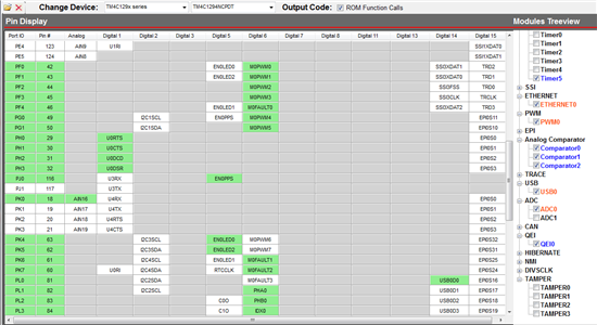
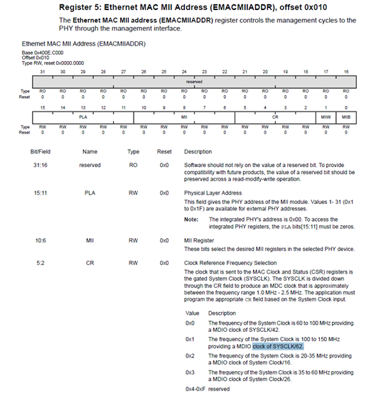
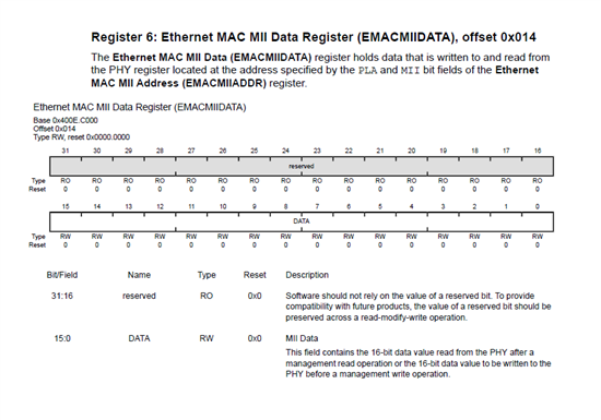
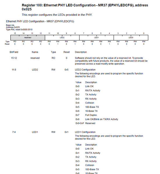
When PWM0 - M0PWM0,1 & M0PWM6,7 pins are enabled & ETH0 is also enabled EN0LED 0-2 become orphaned GPIO pins, seemingly non routable to any other free GPIO pins.
Regarding the EK-TM4C1294XL circuit board when PWM0-M0PWM0,1 & Fault inputs M0Fault1 is made enabled;
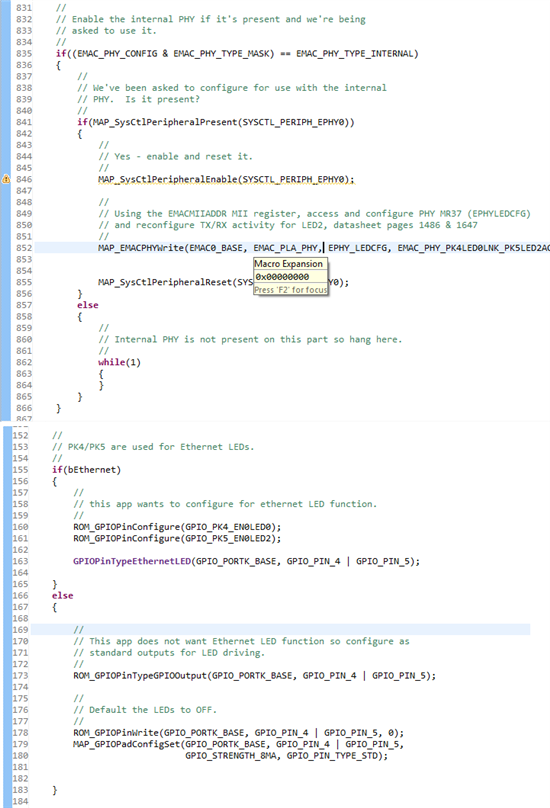
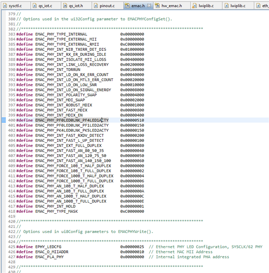
When PWM0 - M0PWM6 or M0PWM7 are disabled M0PWM0,1 enabled and M0Fault0 & 1 are enabled. Then EN0LED1 PF4 pin 46 & EN0LED0 PF0 pin 42, circuit trace must be cut and rerouted to PK5 pin 62, PK4 pin 63 respectively. EN0LED1 blink re-program as EN0LED2 blink thereby freeing up PK6 pin 61 GPIO input for M0Fault1, PF0-pin42 for M0PWM0 and PF4-pin46 for M0PWM3.
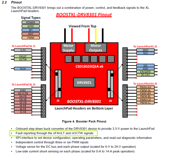
Appears the DRV801 BP does not conform to the EK-TMC129xl PWM pin assignments as anyone might expect they should. Merely judging the PCB visual layout as being compatible could end up porting mostly billowing smoke.


