This thread has been locked.

If you have a related question, please click the "Ask a related question" button in the top right corner. The newly created question will be automatically linked to this question.

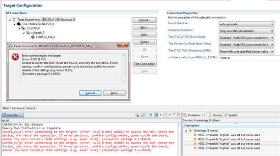
Tiva EK-TM4C1294XL fails to flash during debug with ICDI or JATG.

Guru 55913 points
Other Parts Discussed in Thread: CCSTUDIO, LM3S8971

XM4C1294NCPDT after several memory flashes suddenly decides to no longer transfer bytes at the MPU emulator level. As yet have never flashed any SW or unlocked any GPIO port C JTAG 0:3 however pins C7, C4 have been set as analog comparator input pins. The application is flashing the LED's and talking on UART0 to COM3 and a GUI can connect to the target on the Ethernet.

Anyone have some ideas to what might be happening?

The XDS100V2 passes all loop back tests while the ICDI crashes CCS5.4 upon canceling the failed connection of the DAP though a JTAG connection skips the crash event of (DebugLib.dll). Reinstalled the CCS5.4 Debug server and Stellaris simulator packages did not help. JTAG test  

[Start]

Execute the command:

%ccs_base%/common/uscif/dbgjtag -f %boarddatafile% -rv -o -F inform,logfile=yes -S pathlength -S integrity

[Result]


-----[Print the board config pathname(s)]------------------------------------

C:\Users\BRETT~1.WIN\AppData\Local\.TI\1655298653\
    0\0\BrdDat\testBoard.dat

-----[Print the reset-command software log-file]-----------------------------

This utility has selected a 100- or 510-class product.
This utility will load the adapter 'jioserdesusb.dll'.
The library build date was 'Mar  9 2014'.
The library build time was '22:27:48'.
The library package version is '5.1.450.0'.
The library component version is '35.34.40.0'.
The controller does not use a programmable FPGA.
The controller has a version number of '4' (0x00000004).
The controller has an insertion length of '0' (0x00000000).
This utility will attempt to reset the controller.
This utility has successfully reset the controller.

-----[Print the reset-command hardware log-file]-----------------------------

The scan-path will be reset by toggling the JTAG TRST signal.
The controller is the FTDI FT2232 with USB interface.
The link from controller to target is direct (without cable).
The software is configured for FTDI FT2232 features.
The controller cannot monitor the value on the EMU[0] pin.
The controller cannot monitor the value on the EMU[1] pin.
The controller cannot control the timing on output pins.
The controller cannot control the timing on input pins.
The scan-path link-delay has been set to exactly '0' (0x0000).

-----[The log-file for the JTAG TCLK output generated from the PLL]----------

There is no hardware for programming the JTAG TCLK frequency.

-----[Measure the source and frequency of the final JTAG TCLKR input]--------

There is no hardware for measuring the JTAG TCLK frequency.

-----[Perform the standard path-length test on the JTAG IR and DR]-----------

This path-length test uses blocks of 512 32-bit words.

The test for the JTAG IR instruction path-length succeeded.
The JTAG IR instruction path-length is 4 bits.

The test for the JTAG DR bypass path-length succeeded.
The JTAG DR bypass path-length is 1 bits.

-----[Perform the Integrity scan-test on the JTAG IR]------------------------

This test will use blocks of 512 32-bit words.
This test will be applied just once.

Do a test using 0xFFFFFFFF.
Scan tests: 1, skipped: 0, failed: 0
Do a test using 0x00000000.
Scan tests: 2, skipped: 0, failed: 0
Do a test using 0xFE03E0E2.
Scan tests: 3, skipped: 0, failed: 0
Do a test using 0x01FC1F1D.
Scan tests: 4, skipped: 0, failed: 0
Do a test using 0x5533CCAA.
Scan tests: 5, skipped: 0, failed: 0
Do a test using 0xAACC3355.
Scan tests: 6, skipped: 0, failed: 0
All of the values were scanned correctly.

The JTAG IR Integrity scan-test has succeeded.

-----[Perform the Integrity scan-test on the JTAG DR]------------------------

This test will use blocks of 512 32-bit words.
This test will be applied just once.

Do a test using 0xFFFFFFFF.
Scan tests: 1, skipped: 0, failed: 0
Do a test using 0x00000000.
Scan tests: 2, skipped: 0, failed: 0
Do a test using 0xFE03E0E2.
Scan tests: 3, skipped: 0, failed: 0
Do a test using 0x01FC1F1D.
Scan tests: 4, skipped: 0, failed: 0
Do a test using 0x5533CCAA.
Scan tests: 5, skipped: 0, failed: 0
Do a test using 0xAACC3355.
Scan tests: 6, skipped: 0, failed: 0
All of the values were scanned correctly.

The JTAG DR Integrity scan-test has succeeded.

[End]

Seemingly this behavior occurred after making WatchDog0 and uDMA  peripherals present/sleep in the current configuration. The only call to Port C is made in high nibble binary shown below, we can rule that out.

ROM_GPIOPinTypeComparator(GPIO_PORTC_AHB_BASE, GPIO_PIN_7 | GPIO_PIN_4);

Window7 application logs the crash event: Faulting application name: ccstudio.exe, version: 0.0.0.0, time stamp: 0x4d87abff, Faulting module name: DebugLib.dll_unloaded, version: 0.0.0.0, time stamp: 0x50ec252b Exception code: 0xc0000005 Fault offset: 0x68f8a92d, Faulting process id: 0x1550, Faulting application start time: 0x01cf600d2ef99b47,Faulting application path: D:\CCs54\ccsv5\eclipse\ccstudio.exe, Faulting module path: DebugLib.dll, Report Id: 20bae081-cc01-11e3-bca7-00d0b7062877. 


  • Hello BP101

    Thanks for the details. The usual "suspects" can be ruled out.

    1. JTAG Connection Test uses the BYPASS JTAG Command to check if the JTAG Chain is OK. This is a condition to check if the device on the board is well connected on JTAG. However it does not mean that DAP can be accessed.

    "Seemingly this behavior occurred after making WatchDog0 and uDMA  peripherals present/sleep in the current configuration"

    Can you send a code snapshot of what was additionally done?

    Regards

    Amit

  • Amit, This is worse than leaving the keys inside car, doors locked and motor running. Lol :)

    Agree the DAP is being a DIP!

    The Watchdog0 code was always being asserted with every flash (15-20) times or more but I had forgotten to add the peripheral enable for dog. That was partly to blame for some very odd debug behavior. Possibly (BootLoader) jump past main symbol up to top of memory address as well though (BL) is not in flash memory now. The uDMA peripheral present + same sleep enable as below, no more uDMA code.

    However added back the code to make the entire MPU sleep when no interrupts are occurring but flashed the board successfully many times after that and there is much activity of the MAC/PHY. That suggests no sleep mode here.

    ROM_SysCtlPeripheralEnable(SYSCTL_PERIPH_WDOG0);

    ROM_SysCtlPeripheralSleepEnable(SYSCTL_PERIPH_WDOG0);

    // Initialize the Watchdog timer for a 100ms timeout.  

    IntEnable(INT_WATCHDOG); 

    WatchdogReloadSet(WATCHDOG0_BASE, WATCHDOG_RELOAD_VALUE);   

    WatchdogResetEnable(WATCHDOG0_BASE);   

    WatchdogEnable(WATCHDOG0_BASE);     


  • Might this be an issue with early (DebugLib.dll) reading TM4C (BOOTCFG) register 0x400F.E000:0x1D0 acknowledge CCS5.4 is Go for Debug mode after reading Control bits 0/1?

    The DBG1bit must be 1 and DBG0 must be 0 for debug to be available.

    This register is at reset Default values in loaded firmware.

    CCS5.4, SYS-BIOS 6.35.04.50, TI compiler  v5.1.5

  • Yet another clue in popup message however is not entirely true as the Launch Pad ICDI does a reset and all the LEDS extinguish appears briefly halt for 1-2 seconds. This MPU is on flight 370 path????

  • Hello BP101

    Yes. If the DBG1 is not equal to 1 and DBG0 is not equal to 0, then it would block the JTAG. This is a commit register, so it has to be committed to flash. Else on the next power up the register will revert to the reset value.

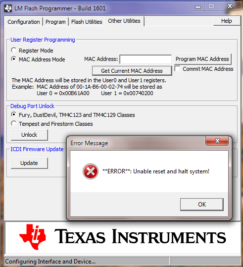
    However you can still run "Unlock Sequence".

    Regards

    Amit

  • Question is what on Earth tripped (BOOTCFG) register bits from the reset values and also commit to flash?

  • Hello BP101,

    I think the only way we can do that now is to unlock the part and reload the code and set a watchpoint on the register access.

    Regards

    Amit

  • Hi Amit,

    This issue may appear related of SWBL posted in this forum please excuse the merge will link it to this post.

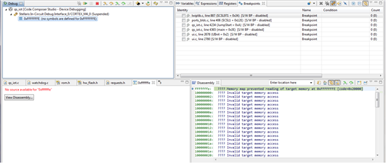
    Works ok now but suspect there is an issue in this register area since the SW boot loader was 4 bytes off in the application target in RSRAM after it first RUNS PC to 0xFFFF.FFFE bypassing (main) symbol at 0x0000.1000.

    Was thinking to commit write EN=1 however the EN bit needs to be 1 at POR and the rule is 1-0 defeats any such write. Data sheet text is not making much sense when a ROM BL is not desired it still executes the PC @0x0000.0004,  EN=1 and moves the SP from flash to 0x0000.0000. Do we execute the first application instruction using the SP or PC?

    If text is correct the APP_BASE set 0x0000.0000 the PC would miss the first 4 instructions though it states it looks for 0xFFFF.FFFF, suspect not always. SWBL appears to be copying the application into SRAM 4 bytes off or the PC is off and Debug merely aligns as it seems to do when doing a move to line (main) with HW break point. Debug often show (BL_Loop) in disassembly window after a CPU warm reset. Was forced to set the AP_BASE back to 0x0000.0000 and obviously overwrite the SWBL. Does the APP_BASE of the application need to be 0x0000.1004 as a work around when a SWBL is installed?

    Oddly in coincidence the text below mentions 0xFFFF.FFFE returns register contents during POR however think that is not always the case when SWBL occupies low Flash memory. I know that to be true if one pulls USB cable during Debug ends.

    The register contents are unaffected by any reset condition except power-on reset, which returns the register contents to 0xFFFF.FFFE for the BOOT Configuration (BOOTCFG) register and 0xFFFF.FFFF for all others.

  • Hello BP101

    We execute the first application instruction using PC @ 0x0000.0004

    The first 4 locations are the SP for the application and do not have a instruction. It is merely a pointer.

    So when a new Application has to be loaded at another offset the APP_BASE would  have the content as SP=APP_BASE and PC=APP_BASE+0x4.

    However when the SWBL was being used there must have been a commit done to the BOOTCFG?

    Regards

    Amit

  •  SWBL was being used there must have been a commit done to the BOOTCFG? Not by me nor can that be found in  (bl_startup_ccs.c). Appearing to confirm issues is in CCCS5.4 (debug_lib.dll). Flash Programmer 6.01 has no issues in repeat flashings, checksums always good. Now starting to see hangs during flash loads in CCS5.4. Most prevalent error, "Unable to Halt the processor". Oddly after deleting then restored the DebugServer.jar and StellarisSimulator.jar . 

    Added a short code piece to insure commit (BOOTCFG) RO register via FMD- DBG=1/0, EN=1. Code single steps but never shows the FMC commit register flag change and the two 16 bit private keys never update the FMC/FLPEKEY registers. There are no functions to be found Tiva library (flash.c) or (sysctrl.c) to commit BOOTCFG register. The odd thing is after this commit was loaded the debug secession once again started same automatic run to address 0xFFFFFFFFE.

     // Commit the ROM (BOOTCFG) register value to nonvolatile flash memory, the POR default. Writes to register FMC/2 using FLPEKEY (0xA442) are ignored. We use a pair of private high and low 16 bit keys committed into flash. Commit FMC insures (BOOTCFG) Debug control bits never lockout the DAP.

    HWREG(FLASH_FMA) = 0x75100000; //(BOOTCFG) address     

    HWREG(FLASH_FMD) = 0xFFFFFFFE; //Insure POR (BOOTCFG) EN=1, DBG=1/0   

    HWREG(FLASH_FLPEKEY) = FLASH_FMC_WRL16KEY;     

    HWREG(FLASH_FMC) = FLASH_FMC_WRH16KEY;      

    HWREG(FLASH_FMC_COMT); //Commit flash

    Amit, Thanks for checking this out!


  • Hello BP101

    Will check it out and send an update.

    Regarda

    Amit

  • Hi Amit,

    I tried flashing Tivaware 5kb SWBL  again this morning using LMF. The Stellaris 4kb SWBL would look for the application interrupt vector table copied to SRAM 0x2000.0000. We would always flash the application above the SWBL to offset 0x0000.1000 for past Stellaris SWBL.  Attempted to allow for a larger Tivaware SWBL and loaded application flash offset 0x0000.1388  or decimal 5k, without the decimal points shown here.

    Seeing the very same results. The SWBL never finds the interrupt vector table of the copied application from flash into low SRAM 0x0000.0000. Relocation of the PC in CCS5.4 debug 0xFFFF.FFFE is not noticed when just the SWBL is loaded hence why I added the (BOOTCFG) lines above posting.

    Once the application offset is flashed the PC is relocating or jumping to address 0xFFFF.FFFE as previously reported, even while using LMFlash with the higher or lower offset application addresses. This happens with or without the added code in the post above.

    When the Tivaware SWBL is step debug in CCS5.4 it appears to be functioning correctly jumping into a reset after failing to find the interrupt vector table or symbol (main) presumably at SRAM 0x2000.0000. Even tried to set the application offset address to 0x0000.1004 getting same results. Either way in my opinion  LMFlash 6.01 being used to load both the SWBL and the application is ruling out CCS5.4 (Debug_server.dll) being the primary suspect.

  • Hello BP101,

    In the sequence mentioned, the last step is a HWREG without any further operator. Can you please clarify?

    HWREG(FLASH_FMC_COMT); //Commit flash

    Secondly, can you elaborate as points 1.2.3. what the steps the SWBL is doing, so that I can have a better picture of the SWBL, since I do not have the source code?

    Regarda

    Amit

  • BP101 said:
    interrupt vector table copied to SRAM 0x0000.0000.

    Does not SRAM begin (as you later note) @ 0x2000.0000?  I've not known SRAM to reside @ 0x0000.0000 - as you imply!

    Earlier you chose a, "purely decimal location" of 2000 - while the MCU preferred 2K binary - 2048.  And above post now speaks to, "flash offset"  0x0000.1388  or decimal 5k.   That 0000.1388 is extremely suspect! 

    Seems that poster's penchant for "decimal" (earlier, pronounced cured) remains alive/well - perhaps entrenched...

  • @Amit, last step is setting the commit bit which the text states need be the very last step performed in the sequence.

    Not sure what you mean by 1.2.3 however the SWBL is included in the EK- TM4C1294Xl launch pad project and support files. Method of setting the (BOOTCFG) registers page numbers are in the green text. Hard to believe no one has tested Tivaware BL with TM4C1294 processor. The BL concept of coping the application from Flash to Scram has been working on Stellaris LM3S8971 for quite some time without ever moving the PC to 0xFFFF.FFFE. The (bl_config.h) is mostly defaults. 0245.bl_config.h

    5658.bl_startup_ccs.s

    BTW: The frame work for this application project came from (qs_iot) as a base which added numerous functions unto.

    @CB1 inferring the APP_BASE 0x0000.0000 starts at 0x2000.0000. You are correct, somewhat loosely worded in that context. That application base address was confirmed several post above to be 0x0000.1000 for the 4kb v10636 Stellaris BL. The Tivaware BL is taking up 5KB figured why not give it some breathing room insuring not to overload SWBL with parts of the applications huge interrupt vector map in Flash. That required modifying the (bl_config.h) entries and applications base address to reflect one another. Suspect the (BOOTCFG) register is being read during POR setting the PC incorrectly reflecting the actual RO register set by alternate register assignment. 

  • Hello BP101

    The HWREG is not setting the commit bit but attempting doing a read operation of the address 0x8.

    Regards

    Amit

  • See what you mean FMC bit 8 read. Ended up that way because compiler error stated (FMC &= CMT) must be a modifiable value. Just tried (FMC | CMT) works ok. Text states to take some care with the commit register to insure only one bit is set any given access. See the REG68 text page at bottom has directions to the instructions of how to unlock the processor.  


  • Hello BP101,

    Can you please send the value for the define in the sequence as the define FLASH_FMC_WRL16KEY and FLASH_FMC_WRH16KEY are not there in the TIVAWare 2.1.0

    Also this code piece is to be loaded into Flash and executed or to be loaded in SRAM and executed?

    Regards

    Amit

  • Hi Amit,  Have been flashing APP_BASE 0x0000.0000 application will not run from the offset using the SWBL. Good point you bring up,  relied on SWBL to copy the application form flash into SRAM and execute the code from there. The TM4C must be executing the application from flash memory, PC _INIT 0x0000.0000?

    You can create any access key values assume they need to match H/L.

    #define FLASH_FMC_WRL16KEY      0x0000DAD0

    #define FLASH_FMC_WRH16KEY      0xDAD00000


  • Hi Amit,

    Did some more work on this issue but still getting same results. Adjusted the APP_BASE 0x0000.1400 and moved the (BOOTCFG) code into the SWBL, selected by (bl_config.h). Forum posts are discussing ROM-BL and doesn't seem to fit what this issues is about. Wonder if that ROMBL code gets deleted when unlocking the DAP? Exosite writes their metadata CIK key stored in flash later written to EEROM which gets erased during LMFlash unlocking the DAP along with flash user registers.

    Now (presumably) having issues writing the EEROM with a new CIK which is being configured in the API using (eerom.c). The application never checks if an error occurs during the EEROM initialization, only later R/W cycles are tested for several fault level though the API fault handler never flags a fault blinking LED. Started having issues with the CIK shortly after the first unlocking of the DAP and now several more occurrences of unlocking the DAP have taken place and no CIK is found in the EEROM when the API checks for one.


  • That blue (highlight) is annoying - camouflages rather than illuminates...

    BP101 said:
    Wonder if that ROMBL code gets deleted when unlocking the DAP?

    ROM getting deleted - not too likely - mon ami.  (and you must know this...)

  • Keep searching for where in CCS5 to turn off that annoying blue blinding background, not to be found in syntax colors.

    That word ROM added to BL in (BOOTCFG) searches text scarcely mentioned within the halls of Montezuma. Yet one questions how changes to any such stored ROM code could be easily made when issues arise. In my opinion EEROM would be the more logical place to store a ROMBL and in such EE became sling shot over UV. Many tears days of ROM burns gone amuck, landfills overflowing with Gemini, Apollo missions desire to one day reach the stars.

  • Cure for that annoying (CCS5 featured, blinding blue) clearly is IAR.  (or Keil)  Big boy/gurl IDE then accommodates M0 and M3 devices from (strangely) many vendors - and supports the faster, more advanced, pin-saving SWD.  

    Many/most (Rom enabled) MCUs employ a masked ROM - which does not accommodate easy (or any) change.  For your development - you can always use Flash-based boot-loader - and then change to your heart's content.  

    Haven't seen/smelled any (recent) smoke from your basement lab - nor seen further, "House for Sale" signs sprout anew - your block.  Can only mean that all BLDC motor development has stalled - as you "ease" between working (yet abandoned) M3 and battle this E-netted, attention-diverting, M4 replacement...