This thread has been locked.

If you have a related question, please click the "Ask a related question" button in the top right corner. The newly created question will be automatically linked to this question.

Write to Port B showing up on Port C and Port D

Other Parts Discussed in Thread: EK-TM4C123GXL

Hello,

I am trying to write a program based around the Kentec EB-LM4F120-L35.  Basically the program grabs data over CAN and SPI and then updates either updates the screen based on the received values and/or write data back out over CAN.

Right now I cannot get my SSI peripheral to work after I call some of the Kentec320x240x16_ssd2119_8bit.c functions for the touchscreen.  Although I am still not sure what is going on, I noticed that when the function "Kentec320x240x16_SSD2119RectFill()" gets called I get some random data popping up on the pins I have dedicated to SSI (PD0-CLK, PD1-FSS, PD2-RX, PD3-TX).  I have retested the code without making any GRLIB or Kentec320x240x16_ssd2119_8bit.c calls and SSI functions exactly as expected.

I have used a logic analyzer to track down one of the many places random data is popping up on PD1 (which is FSS) and it makes no sense to me why this is happening.  Here are the line of code causing the spurious data to pop up:

HWREG(LCD_CS_BASE + GPIO_O_DATA + (LCD_CS_PIN << 2)) = 0;

And here are the definitions referenced in the line of code:

#define LCD_CS_BASE              GPIO_PORTA_BASE
#define GPIO_O_DATA               0x00000000 // GPIO Data
#define LCD_CS_PIN                  GPIO_PIN_7
#define GPIO_PIN_7                   0x00000080 // GPIO pin 7

This is happening with other similar HWREG calls too.  I have also confirmed that all the applicable registers are reading as they should (no writes to GPIO Port D or SSI1).

Based on the provided code snippet and short summary can anyone give me some guidance on what to investigate next?  My only guess is that the code snippet above is somehow writing data to incorrect registers, but then again the registers I have suspected are not showing anything wrong.  I have also attached my logic analyzer trace.

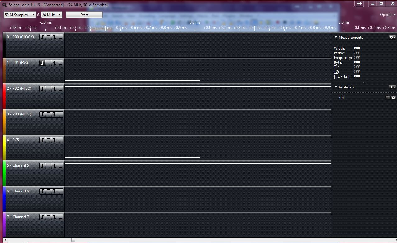
Any help is appreciated!

  • Hello Matt

    Can you please check the GPIO's PCTL and AFSEL register values to make sure that the correct GPIO is configured.

    For a GPIO to be used as a GPIO : AFSEL for the bit should be 0 and PCTL is a don't care

    For a GPIO to be used as a Peripheral Pin: AFSEL for the bit should be 1 and PCTL should map to the Signal Description Table Value in paranthesis.

    Regards

    Amit

  • Amit,

    I was able to verify that the registers were set correctly both for Port D (SSI) as well as Ports A and B (Used by the display driver).

    Another interesting piece of evidence I have come across is if I switch my code around so that SSI gets initalized before anything relating to my display driver I do not get the random data popping up on any of my Port D (SSI) pins, but SSI still does not work.  When I say it still does not work, I mean that when I initialize the peripheral, I also send some initialization messages to my device and successfully transmit and receive.  But I am not able to transmit at all after I initialize my display which I have verified again is ONLY modifying Port A and Port B registers.  So again, it seems as if either my SSI peripheral or Port D GPIO pins are inadvertently getting modified by my display driver.

    On a hardware note, I have verified this is a problem occurs both when my screen is plugged into the launchpad as well as when nothing is plugged into the launchpad.

    On other possibility I thought of was that I am writing Stellaris code and flashing it onto a Tiva micro.  I know that Tiva is supposed to be backwards compatible but I am going to retry with a Stellaris launchpad instead to see if the problem persists.

    Thank you for your help!

    Matt

  • Amit,

    I was able to verify the issue exists with both my Stellaris Launchpad and my Tiva Launchpad.

    I also just tried some old working code.  The only difference between the old code is an extra canvas widget from grlib that I am trying to first initialize and then update on the fly.  So after this type of "A-B-A" test I can be sure this error is somehow coming from my calls to grlib.  I am starting to think that my display driver may be the culprit and may be overwriting unintended registers.

    I'll see what I can find regarding the way I am setting up my widget tree specifically.

    Matt

  • Hello Matt

    I suspect the same as well. Can you take the register dump of the Ports from address offset 0x400 to 0x440 and then 0x500 to 0x540 for the problematic port for TIVA

    We can then cross check what is getting programmed.

    Regards

    Amit

  • Amit,

    Since my last post I was able to hone in on the location (or possibly just one of the locations) this problem is occurring.  I will first provide a summary of how I drilled down to find the location of where my SPI bus may possibly be getting disabled:

    Here is the main framework of my code:

    int
    main(void)
    {
    	//*****************************************************************************
    	//
    	// Global variables for whole project
    	//
    	//*****************************************************************************
    
    	//
    	// uint8_t buttons is used to store current button states to be sent out to the
    	// CAN FIFO.  The CAN library requires that the address of this variable be
    	// passed via the CAN message object.
    	//
    	uint16_t buttons = 0;
    	uint16_t buttonsRemapped = 0;
    
    	//
    	// uint8_t flags is used as a temporary variable in Wheel_MAIN.c to store the
    	// received timer interrupt flags.
    	//
    	uint8_t flags = 0;
    
        //
        // Set the clocking to run directly from the external crystal/oscillator.
        // TODO: The SYSCTL_XTAL_ value must be changed to match the value of the
        // crystal on your board.
        //
        SysCtlClockSet(SYSCTL_SYSDIV_2_5 | SYSCTL_USE_PLL | SYSCTL_OSC_MAIN | SYSCTL_XTAL_16MHZ);
    
        SSIInitialize();
        GraphicsInitialize();
        Timer0Init();
        ButtonsInitialize();
        CANInitialize();
    
        while(1)
        {
        	flags = timerGetFlags();
        	if((flags & FLAG_10MS) == FLAG_10MS)
        	{
        		buttons = ButtonDebounce();
        		buttonsRemapped = ButtonRemap(buttons);
        		CANTxButtons((uint8_t *)&buttonsRemapped);
        	}
    
        	LCDUpdate();
            CANDataHandler();
        }
    }

    Now only focus on the two initialization functions SSIInitialize() and GraphicsInitialize(). SSIInitialize() goes through and properly initializes the SSI1 peripheral and successfully sends a configuration packet to the GPIO expander I am using. Here is the code contained in SSIInitialize():

    void
    SSIInitialize(void)
    {
    	//
    	// Initialize local variables for function
    	//
    	unsigned long pui32DataTx[NUM_TX_BYTES_SSI_DATA];
    	unsigned long pui32DataRx[NUM_RX_BYTES_SSI_DATA];
        uint32_t ui32Index;
    
    
        //
        // The SSI0 peripheral must be enabled for use.
        //
        SysCtlPeripheralEnable(SYSCTL_PERIPH_SSI1);
    
        //
        // For this project SSI0 is used with PortD[3:1] because those
        // are the launchpad pins the GPIO expander connects to.
        // GPIO port D needs to be enabled so these pins can be used.
        //
        SysCtlPeripheralEnable(SYSCTL_PERIPH_GPIOD);
    
        //
        // Configure the pin muxing for SSI0 functions on port D0, D2, D3, and D1.
        //		SSI1Clk - PD0
        //		SSI1Fss - PD1
        //		SSI1Rx  - PD2
        //		SSI1Tx  - PD3
        //
        GPIOPinConfigure(GPIO_PD0_SSI1CLK);
        GPIOPinConfigure(GPIO_PD1_SSI1FSS);
        GPIOPinConfigure(GPIO_PD2_SSI1RX);
        GPIOPinConfigure(GPIO_PD3_SSI1TX);
    
        //
        // Configure the GPIO settings for the SSI pins.  This function also gives
        // control of these pins to the SSI hardware.
        // The pins are assigned as follows:
        //      PD0 - SSI1Clk
        //      PD1 - SSI1Fss
        //      PD2 - SSI1Rx
        //      PD3 - SSI1Tx
        //
        GPIOPinTypeSSI(GPIO_PORTD_BASE, GPIO_PIN_0 | GPIO_PIN_1 | GPIO_PIN_2 |
                       GPIO_PIN_3);
    
        //
        // Configure and enable the SSI port for SPI master mode.  Use SSI1,
        // system clock supply, idle clock level low and active low clock in
        // freescale SPI mode, master mode, 1MHz SSI frequency, and 8-bit data.
        // SSI mode 3 allows FSS to stay low for multiple bytes being clocked
        // out.  The MCP23S17 GPIO expander requires this
        //
        SSIConfigSetExpClk(SSI1_BASE, SysCtlClockGet(), SSI_FRF_MOTO_MODE_3,
                           SSI_MODE_MASTER, 5000000, 8);
    
        //
        // Enable the SSI1 peripheral module.
        //
        SSIEnable(SSI1_BASE);
    
        //
    	// Read any residual data from the SSI port.  This makes sure the receive
    	// FIFOs are empty, so we don't read any unwanted junk.  This is done here
    	// because the SPI SSI mode is full-duplex, which allows you to send and
    	// receive at the same time.  The SSIDataGetNonBlocking function returns
    	// "true" when data was returned, and "false" when no data was returned.
    	// The "non-blocking" function checks if there is any data in the receive
    	// FIFO and does not "hang" if there isn't.
    	//
    	while(SSIDataGetNonBlocking(SSI1_BASE, &pui32DataRx[0]))
    	{
    	}
    
    	//
    	// Initialize the data to send. This packet will configure the MCP23S17
    	//
    	pui32DataTx[0] = 0x40;	// MCP23S17 opcode write mode, address 0x00
    	pui32DataTx[1] = 0x0A;	// MCP23S17 register address for IOCON
    	pui32DataTx[2] = 0x20;  // MCP23S17 configuration data
    
    	//
    	// Disable Interrupts
    	//
    	IntMasterDisable();
    
    	//
    	// Send 3 bytes of data.
    	//
    	for(ui32Index = 0; ui32Index < NUM_TX_BYTES_SSI_DATA; ui32Index++)
    	{
    
    		//
    		// Send the data using the "blocking" put function.  This function
    		// will wait until there is room in the send FIFO before returning.
    		// This allows you to assure that all the data you send makes it into
    		// the send FIFO.
    		//
    		SSIDataPut(SSI1_BASE, pui32DataTx[ui32Index]);
    	}
    
    	//
    	// Wait until SSI0 is done transferring all the data in the transmit FIFO.
    	//
    	while(SSIBusy(SSI1_BASE))
    	{
    	}
    
    	while(SSIDataGetNonBlocking(SSI1_BASE, &pui32DataRx[0]))
    	{
    	}
    
    	//
    	// Enable Interrupts
    	//
    	IntMasterEnable();
    }

    After the SSIInitialize() function runs, I then use another function named SSIButtonRead() to send data read packets to the GPIO expander.  This function normally works fine until GraphicsInitialize() gets called.  I could not figure out by reading the code what part of GraphicsInitialize() could possibly be affecting my SSI1 peripheral so I started sticking the following two lines of code into the various parts of GraphicsInitialize() until I could make it fail:

    HWREG(GPIO_PORTB_BASE + GPIO_O_DATA + (0xff << 2)) = 0x00BA;
    SSIButtonRead()

    I tested for failure by looking at the scope output of the SPI pins.  I was able to make the function fail right after the function named Kentec320x240x16_SSD2119Init() was called shown below:

    void
    GraphicsInitialize(void)
    {
        //
        // Initialize the display driver.
        //
        Kentec320x240x16_SSD2119Init();
    
        //
        // Initialize the graphics context.
        //
        GrContextInit(&sContext, &g_sKentec320x240x16_SSD2119);
    
        //
        // Add the first panel to the widget tree. Display WR splash screen.
        //
    
        WidgetAdd(WIDGET_ROOT, (tWidget *)(g_psPanels + 0));
        WidgetPaint((tWidget *)(g_psPanels + 0));
        WidgetMessageQueueProcess();
        SysCtlDelay(20000000);
    
        //
        // Add the second panel to the widget tree.  Display main parameter screen.
        //
        WidgetRemove((tWidget *)(g_psPanels + 0));
        WidgetAdd(WIDGET_ROOT, (tWidget *)(g_psPanels + 1));
        WidgetPaint((tWidget *)(g_psPanels + 1));
        WidgetMessageQueueProcess();
    }

    I then opened up Kentec320x240x16_SSD2119Init(), which is part of a driver which I did not write, and injected the same two lines of code various places.  I found that the failure occurred right after a function named InitGPIOLCDInterface(ulClockMS) was executed.  The Kentec320x240x16_SSD2119Init() function is shown here:

    void
    Kentec320x240x16_SSD2119Init(void)
    {
        unsigned long ulClockMS, ulCount;
    
        //
        // Get the current processor clock frequency.
        //
        ulClockMS = SysCtlClockGet() / (3 * 1000);
    
    	//
        // Enable the GPIO peripherals used to interface to the SSD2119.
        //
    	SysCtlPeripheralEnable(LCD_DATAH_PERIPH);
        SysCtlPeripheralEnable(LCD_DC_PERIPH);
        SysCtlPeripheralEnable(LCD_RD_PERIPH);
        SysCtlPeripheralEnable(LCD_WR_PERIPH);
    //    ROM_SysCtlPeripheralEnable(LCD_RST_PERIPH);
        SysCtlPeripheralEnable(LCD_CS_PERIPH);
        //SysCtlPeripheralEnable(LCD_BACKLIGHT_PERIPH);
    
        //
        // Perform low level interface initialization depending upon how the LCD
        // is connected to the Stellaris microcontroller.  This varies depending
        // upon the daughter board connected it is possible that a daughter board
        // can drive the LCD directly rather than via the basic GPIO interface.
        //
            {
                //
                // Initialize the GPIOs used to interface to the LCD controller.
                //
                InitGPIOLCDInterface(ulClockMS);
            }
    
        //
        // Enter sleep mode (if we are not already there).
        //
        WriteCommand(SSD2119_SLEEP_MODE_REG);
        WriteData(0x0001);
    
        //
        // Set initial power parameters.
        //
        WriteCommand(SSD2119_PWR_CTRL_5_REG);
        WriteData(0x00BA);
        WriteCommand(SSD2119_VCOM_OTP_1_REG);
        WriteData(0x0006);
    
        //
        // Start the oscillator.
        //
        WriteCommand(SSD2119_OSC_START_REG);
        WriteData(0x0001);
    
        //
        // Set pixel format and basic display orientation (scanning direction).
        //
        WriteCommand(SSD2119_OUTPUT_CTRL_REG);
        WriteData(0x30EF);
        WriteCommand(SSD2119_LCD_DRIVE_AC_CTRL_REG);
        WriteData(0x0600);
    
        //
        // Exit sleep mode.
        //
        WriteCommand(SSD2119_SLEEP_MODE_REG);
        WriteData(0x0000);
    
        //
        // Delay 30mS
        //
        SysCtlDelay(30 * ulClockMS);
    
        //
        // Configure pixel color format and MCU interface parameters.
        //
        WriteCommand(SSD2119_ENTRY_MODE_REG);
        WriteData(ENTRY_MODE_DEFAULT);
    
        //
        // Enable the display.
        //
        WriteCommand(SSD2119_DISPLAY_CTRL_REG);
        WriteData(0x0033);
    
        //
        // Set VCIX2 voltage to 6.1V.
        //
        WriteCommand(SSD2119_PWR_CTRL_2_REG);
        WriteData(0x0005);
    
        //
        // Configure gamma correction.
        //
        WriteCommand(SSD2119_GAMMA_CTRL_1_REG);
        WriteData(0x0000);
        WriteCommand(SSD2119_GAMMA_CTRL_2_REG);
        WriteData(0x0400);
        WriteCommand(SSD2119_GAMMA_CTRL_3_REG);
        WriteData(0x0106);
        WriteCommand(SSD2119_GAMMA_CTRL_4_REG);
        WriteData(0x0700);
        WriteCommand(SSD2119_GAMMA_CTRL_5_REG);
        WriteData(0x0002);
        WriteCommand(SSD2119_GAMMA_CTRL_6_REG);
        WriteData(0x0702);
        WriteCommand(SSD2119_GAMMA_CTRL_7_REG);
        WriteData(0x0707);
        WriteCommand(SSD2119_GAMMA_CTRL_8_REG);
        WriteData(0x0203);
        WriteCommand(SSD2119_GAMMA_CTRL_9_REG);
        WriteData(0x1400);
        WriteCommand(SSD2119_GAMMA_CTRL_10_REG);
        WriteData(0x0F03);
    
        //
        // Configure Vlcd63 and VCOMl.
        //
        WriteCommand(SSD2119_PWR_CTRL_3_REG);
        WriteData(0x0007);
        WriteCommand(SSD2119_PWR_CTRL_4_REG);
        WriteData(0x3100);
    
        //
        // Set the display size and ensure that the GRAM window is set to allow
        // access to the full display buffer.
        //
        WriteCommand(SSD2119_V_RAM_POS_REG);
        WriteData((LCD_VERTICAL_MAX-1) << 8);
        WriteCommand(SSD2119_H_RAM_START_REG);
        WriteData(0x0000);
        WriteCommand(SSD2119_H_RAM_END_REG);
        WriteData(LCD_HORIZONTAL_MAX-1);
        WriteCommand(SSD2119_X_RAM_ADDR_REG);
        WriteData(0x00);
        WriteCommand(SSD2119_Y_RAM_ADDR_REG);
        WriteData(0x00);
    
        //
        // Clear the contents of the display buffer.
        //
        WriteCommand(SSD2119_RAM_DATA_REG);
        for(ulCount = 0; ulCount < (320 * 240); ulCount++)
        {
            WriteData(0x0000);
        }
    }

     I then opened up the InitGPIOLCDInterface() function and injected the lines of code various places again and found that the failure occurred right after the following function:

     GPIOPinTypeGPIOOutput(LCD_DATAH_BASE, LCD_DATAH_PINS);

    Where LCD_DATAH_BASE is defined as GPIO_PORTB_BASE (0x40005000) and LCD_DATAH_PINS is defined as 0xff

    Here is the location of that function within the InitGPIOLCDInterface() function with my test code inserted (I no longer the line HWREG(GPIO_PORTB_BASE + GPIO_O_DATA + (0xff << 2)) = 0x00BA to make the SPI bus fail, it just wouldn't output anything right after  GPIOPinTypeGPIOOutput(LCD_DATAH_BASE, LCD_DATAH_PINS) was called)

    static void
    InitGPIOLCDInterface(unsigned long ulClockMS)
    {
        //
        // Configure the pins that connect to the LCD as GPIO outputs.
        //
        SSIButtonRead();
        GPIOPinTypeGPIOOutput(LCD_DATAH_BASE, LCD_DATAH_PINS);
        SSIButtonRead();
    
        GPIOPinTypeGPIOOutput(LCD_DC_BASE, LCD_DC_PIN);
        GPIOPinTypeGPIOOutput(LCD_RD_BASE, LCD_RD_PIN);
        GPIOPinTypeGPIOOutput(LCD_WR_BASE, LCD_WR_PIN);
        GPIOPinTypeGPIOOutput(LCD_CS_BASE, LCD_CS_PIN);
    //    GPIOPinTypeGPIOOutput(LCD_BACKLIGHT_BASE, LCD_BACKLIGHT_PIN);
    //    GPIOPinTypeGPIOOutput(LCD_RST_BASE, LCD_RST_PIN);LCD_BACKLIGHT_BASE
    
        //
        // Set the LCD control pins to their default values.  This also asserts the
        // LCD reset signal.
        //
        GPIOPinWrite(LCD_CS_BASE, LCD_CS_PIN, LCD_CS_PIN);
        GPIOPinWrite(LCD_DATAH_BASE, LCD_DATAH_PINS, 0x00);
        GPIOPinWrite(LCD_DC_BASE, LCD_DC_PIN, 0x00);
        GPIOPinWrite(LCD_RD_BASE, LCD_RD_PIN, LCD_RD_PIN);
        GPIOPinWrite(LCD_WR_BASE, LCD_WR_PIN, LCD_WR_PIN);
    //    GPIOPinWrite(LCD_RST_BASE, LCD_RST_PIN, 0x00);
    	GPIOPinWrite(LCD_CS_BASE, LCD_CS_PIN, 0);
    
        //
        // Delay for 1ms.
        //
        SysCtlDelay(ulClockMS);
    
        //
        // Deassert the LCD reset signal.
        //
    //    GPIOPinWrite(LCD_RST_BASE, LCD_RST_PIN, LCD_RST_PIN);
    
        //
        // Delay for 1ms while the LCD comes out of reset.
        //
        SysCtlDelay(ulClockMS);
    }

    At this point I cannot for the life of me figure out why the function GPIOPinTypeGPIOOutput(LCD_DATAH_BASE, LCD_DATAH_PINS) could be affecting anything with the SSI1 peripheral.  I analyzed the GPIO registers for port B and port D as well as the SSI1 registers before and after this function was executed and found nothing wrong.  The register output files are attached from before and after.  Is there possibly some sort of errata that I am missing regarding this issue?

    Keep in mind that I am pretty sure this is one occurrence of many when a function involving Port B knocks out the SSI1 peripheral, but my thought is that if I can figure out the cause of one instance I should be able to solve the problem for the rest.

    ****BEFORE FUNCTION CALL****
    
    521177 14
    R GPIO_PORTA_GPIO_DATA 0x0000000B 0x00000000
    R GPIO_PORTA_GPIO_DIR 0x0000000B 0x00000000
    R GPIO_PORTA_GPIO_IS 0x0000000B 0x00000000
    R GPIO_PORTA_GPIO_IBE 0x0000000B 0x00000000
    R GPIO_PORTA_GPIO_IEV 0x0000000B 0x00000000
    R GPIO_PORTA_GPIO_IM 0x0000000B 0x00000000
    R GPIO_PORTA_GPIO_RIS 0x0000000B 0x00000000
    R GPIO_PORTA_GPIO_MIS 0x0000000B 0x00000000
    R GPIO_PORTA_GPIO_ICR 0x0000000B 0x00000000
    R GPIO_PORTA_GPIO_AFSEL 0x0000000B 0x00000000
    R GPIO_PORTA_GPIO_DR2R 0x0000000B 0x000000FF
    R GPIO_PORTA_GPIO_DR4R 0x0000000B 0x00000000
    R GPIO_PORTA_GPIO_DR8R 0x0000000B 0x00000000
    R GPIO_PORTA_GPIO_ODR 0x0000000B 0x00000000
    R GPIO_PORTA_GPIO_PUR 0x0000000B 0x00000000
    R GPIO_PORTA_GPIO_PDR 0x0000000B 0x00000000
    R GPIO_PORTA_GPIO_SLR 0x0000000B 0x00000000
    R GPIO_PORTA_GPIO_DEN 0x0000000B 0x00000000
    R GPIO_PORTA_GPIO_LOCK 0x0000000B 0x00000001
    R GPIO_PORTA_GPIO_CR 0x0000000B 0x000000FF
    R GPIO_PORTA_GPIO_AMSEL 0x0000000B 0x00000000
    R GPIO_PORTA_GPIO_PCTL 0x0000000B 0x00222211
    R GPIO_PORTA_GPIO_ADCCTL 0x0000000B 0x00000000
    R GPIO_PORTA_GPIO_DMACTL 0x0000000B 0x00000000
    R GPIO_PORTA_GPIO_SI 0x0000000B 0x00000000
    R GPIO_PORTB_GPIO_DATA 0x0000000B 0x00000000
    R GPIO_PORTB_GPIO_DIR 0x0000000B 0x00000000
    R GPIO_PORTB_GPIO_IS 0x0000000B 0x00000000
    R GPIO_PORTB_GPIO_IBE 0x0000000B 0x00000000
    R GPIO_PORTB_GPIO_IEV 0x0000000B 0x00000000
    R GPIO_PORTB_GPIO_IM 0x0000000B 0x00000000
    R GPIO_PORTB_GPIO_RIS 0x0000000B 0x00000000
    R GPIO_PORTB_GPIO_MIS 0x0000000B 0x00000000
    R GPIO_PORTB_GPIO_ICR 0x0000000B 0x00000000
    R GPIO_PORTB_GPIO_AFSEL 0x0000000B 0x00000000
    R GPIO_PORTB_GPIO_DR2R 0x0000000B 0x000000FF
    R GPIO_PORTB_GPIO_DR4R 0x0000000B 0x00000000
    R GPIO_PORTB_GPIO_DR8R 0x0000000B 0x00000000
    R GPIO_PORTB_GPIO_ODR 0x0000000B 0x00000000
    R GPIO_PORTB_GPIO_PUR 0x0000000B 0x00000000
    R GPIO_PORTB_GPIO_PDR 0x0000000B 0x00000000
    R GPIO_PORTB_GPIO_SLR 0x0000000B 0x00000000
    R GPIO_PORTB_GPIO_DEN 0x0000000B 0x00000000
    R GPIO_PORTB_GPIO_LOCK 0x0000000B 0x00000001
    R GPIO_PORTB_GPIO_CR 0x0000000B 0x000000FF
    R GPIO_PORTB_GPIO_AMSEL 0x0000000B 0x00000000
    R GPIO_PORTB_GPIO_PCTL 0x0000000B 0x00003300
    R GPIO_PORTB_GPIO_ADCCTL 0x0000000B 0x00000000
    R GPIO_PORTB_GPIO_DMACTL 0x0000000B 0x00000000
    R GPIO_PORTB_GPIO_SI 0x0000000B 0x00000000
    R GPIO_PORTD_GPIO_DATA 0x0000000B 0x0000000F
    R GPIO_PORTD_GPIO_DIR 0x0000000B 0x00000000
    R GPIO_PORTD_GPIO_IS 0x0000000B 0x00000000
    R GPIO_PORTD_GPIO_IBE 0x0000000B 0x00000000
    R GPIO_PORTD_GPIO_IEV 0x0000000B 0x00000000
    R GPIO_PORTD_GPIO_IM 0x0000000B 0x00000000
    R GPIO_PORTD_GPIO_RIS 0x0000000B 0x0000000F
    R GPIO_PORTD_GPIO_MIS 0x0000000B 0x00000000
    R GPIO_PORTD_GPIO_ICR 0x0000000B 0x00000000
    R GPIO_PORTD_GPIO_AFSEL 0x0000000B 0x0000000F
    R GPIO_PORTD_GPIO_DR2R 0x0000000B 0x000000FF
    R GPIO_PORTD_GPIO_DR4R 0x0000000B 0x00000000
    R GPIO_PORTD_GPIO_DR8R 0x0000000B 0x00000000
    R GPIO_PORTD_GPIO_ODR 0x0000000B 0x00000000
    R GPIO_PORTD_GPIO_PUR 0x0000000B 0x00000000
    R GPIO_PORTD_GPIO_PDR 0x0000000B 0x00000000
    R GPIO_PORTD_GPIO_SLR 0x0000000B 0x00000000
    R GPIO_PORTD_GPIO_DEN 0x0000000B 0x0000000F
    R GPIO_PORTD_GPIO_LOCK 0x0000000B 0x00000001
    R GPIO_PORTD_GPIO_CR 0x0000000B 0x0000007F
    R GPIO_PORTD_GPIO_AMSEL 0x0000000B 0x00000000
    R GPIO_PORTD_GPIO_PCTL 0x0000000B 0x00002222
    R GPIO_PORTD_GPIO_ADCCTL 0x0000000B 0x00000000
    R GPIO_PORTD_GPIO_DMACTL 0x0000000B 0x00000000
    R GPIO_PORTD_GPIO_SI 0x0000000B 0x00000000
    R SSI1_SSI_CR0 0x0000000B 0x000007C7
    R SSI1_SSI_CR1 0x0000000B 0x00000002
    R SSI1_SSI_DR 0x0000000B 0x000000FF
    R SSI1_SSI_SR 0x0000000B 0x00000003
    R SSI1_SSI_CPSR 0x0000000B 0x00000002
    R SSI1_SSI_IM 0x0000000B 0x00000000
    R SSI1_SSI_RIS 0x0000000B 0x00000008
    R SSI1_SSI_MIS 0x0000000B 0x00000000
    R SSI1_SSI_ICR 0x0000000B 0x00000000
    R SSI1_SSI_DMACTL 0x0000000B 0x00000000
    R SSI1_SSI_CC 0x0000000B 0x00000000
    
    
    ****AFTER FUNCTION CALL***
    
    521177 14
    R GPIO_PORTA_GPIO_DATA 0x0000000B 0x00000000
    R GPIO_PORTA_GPIO_DIR 0x0000000B 0x00000000
    R GPIO_PORTA_GPIO_IS 0x0000000B 0x00000000
    R GPIO_PORTA_GPIO_IBE 0x0000000B 0x00000000
    R GPIO_PORTA_GPIO_IEV 0x0000000B 0x00000000
    R GPIO_PORTA_GPIO_IM 0x0000000B 0x00000000
    R GPIO_PORTA_GPIO_RIS 0x0000000B 0x00000000
    R GPIO_PORTA_GPIO_MIS 0x0000000B 0x00000000
    R GPIO_PORTA_GPIO_ICR 0x0000000B 0x00000000
    R GPIO_PORTA_GPIO_AFSEL 0x0000000B 0x00000000
    R GPIO_PORTA_GPIO_DR2R 0x0000000B 0x000000FF
    R GPIO_PORTA_GPIO_DR4R 0x0000000B 0x00000000
    R GPIO_PORTA_GPIO_DR8R 0x0000000B 0x00000000
    R GPIO_PORTA_GPIO_ODR 0x0000000B 0x00000000
    R GPIO_PORTA_GPIO_PUR 0x0000000B 0x00000000
    R GPIO_PORTA_GPIO_PDR 0x0000000B 0x00000000
    R GPIO_PORTA_GPIO_SLR 0x0000000B 0x00000000
    R GPIO_PORTA_GPIO_DEN 0x0000000B 0x00000000
    R GPIO_PORTA_GPIO_LOCK 0x0000000B 0x00000001
    R GPIO_PORTA_GPIO_CR 0x0000000B 0x000000FF
    R GPIO_PORTA_GPIO_AMSEL 0x0000000B 0x00000000
    R GPIO_PORTA_GPIO_PCTL 0x0000000B 0x00222211
    R GPIO_PORTA_GPIO_ADCCTL 0x0000000B 0x00000000
    R GPIO_PORTA_GPIO_DMACTL 0x0000000B 0x00000000
    R GPIO_PORTA_GPIO_SI 0x0000000B 0x00000000
    R GPIO_PORTB_GPIO_DATA 0x0000000B 0x000000C1
    R GPIO_PORTB_GPIO_DIR 0x0000000B 0x000000FF
    R GPIO_PORTB_GPIO_IS 0x0000000B 0x00000000
    R GPIO_PORTB_GPIO_IBE 0x0000000B 0x00000000
    R GPIO_PORTB_GPIO_IEV 0x0000000B 0x00000000
    R GPIO_PORTB_GPIO_IM 0x0000000B 0x00000000
    R GPIO_PORTB_GPIO_RIS 0x0000000B 0x00000000
    R GPIO_PORTB_GPIO_MIS 0x0000000B 0x00000000
    R GPIO_PORTB_GPIO_ICR 0x0000000B 0x00000000
    R GPIO_PORTB_GPIO_AFSEL 0x0000000B 0x00000000
    R GPIO_PORTB_GPIO_DR2R 0x0000000B 0x000000FF
    R GPIO_PORTB_GPIO_DR4R 0x0000000B 0x00000000
    R GPIO_PORTB_GPIO_DR8R 0x0000000B 0x00000000
    R GPIO_PORTB_GPIO_ODR 0x0000000B 0x00000000
    R GPIO_PORTB_GPIO_PUR 0x0000000B 0x00000000
    R GPIO_PORTB_GPIO_PDR 0x0000000B 0x00000000
    R GPIO_PORTB_GPIO_SLR 0x0000000B 0x00000000
    R GPIO_PORTB_GPIO_DEN 0x0000000B 0x000000FF
    R GPIO_PORTB_GPIO_LOCK 0x0000000B 0x00000001
    R GPIO_PORTB_GPIO_CR 0x0000000B 0x000000FF
    R GPIO_PORTB_GPIO_AMSEL 0x0000000B 0x00000000
    R GPIO_PORTB_GPIO_PCTL 0x0000000B 0x00003300
    R GPIO_PORTB_GPIO_ADCCTL 0x0000000B 0x00000000
    R GPIO_PORTB_GPIO_DMACTL 0x0000000B 0x00000000
    R GPIO_PORTB_GPIO_SI 0x0000000B 0x00000000
    R GPIO_PORTD_GPIO_DATA 0x0000000B 0x0000000F
    R GPIO_PORTD_GPIO_DIR 0x0000000B 0x00000000
    R GPIO_PORTD_GPIO_IS 0x0000000B 0x00000000
    R GPIO_PORTD_GPIO_IBE 0x0000000B 0x00000000
    R GPIO_PORTD_GPIO_IEV 0x0000000B 0x00000000
    R GPIO_PORTD_GPIO_IM 0x0000000B 0x00000000
    R GPIO_PORTD_GPIO_RIS 0x0000000B 0x0000000F
    R GPIO_PORTD_GPIO_MIS 0x0000000B 0x00000000
    R GPIO_PORTD_GPIO_ICR 0x0000000B 0x00000000
    R GPIO_PORTD_GPIO_AFSEL 0x0000000B 0x0000000F
    R GPIO_PORTD_GPIO_DR2R 0x0000000B 0x000000FF
    R GPIO_PORTD_GPIO_DR4R 0x0000000B 0x00000000
    R GPIO_PORTD_GPIO_DR8R 0x0000000B 0x00000000
    R GPIO_PORTD_GPIO_ODR 0x0000000B 0x00000000
    R GPIO_PORTD_GPIO_PUR 0x0000000B 0x00000000
    R GPIO_PORTD_GPIO_PDR 0x0000000B 0x00000000
    R GPIO_PORTD_GPIO_SLR 0x0000000B 0x00000000
    R GPIO_PORTD_GPIO_DEN 0x0000000B 0x0000000F
    R GPIO_PORTD_GPIO_LOCK 0x0000000B 0x00000001
    R GPIO_PORTD_GPIO_CR 0x0000000B 0x0000007F
    R GPIO_PORTD_GPIO_AMSEL 0x0000000B 0x00000000
    R GPIO_PORTD_GPIO_PCTL 0x0000000B 0x00002222
    R GPIO_PORTD_GPIO_ADCCTL 0x0000000B 0x00000000
    R GPIO_PORTD_GPIO_DMACTL 0x0000000B 0x00000000
    R GPIO_PORTD_GPIO_SI 0x0000000B 0x00000000
    R SSI1_SSI_CR0 0x0000000B 0x000007C7
    R SSI1_SSI_CR1 0x0000000B 0x00000002
    R SSI1_SSI_DR 0x0000000B 0x000000FF
    R SSI1_SSI_SR 0x0000000B 0x00000003
    R SSI1_SSI_CPSR 0x0000000B 0x00000002
    R SSI1_SSI_IM 0x0000000B 0x00000000
    R SSI1_SSI_RIS 0x0000000B 0x00000008
    R SSI1_SSI_MIS 0x0000000B 0x00000000
    R SSI1_SSI_ICR 0x0000000B 0x00000000
    R SSI1_SSI_DMACTL 0x0000000B 0x00000000
    R SSI1_SSI_CC 0x0000000B 0x00000000
    

  • Sorry to jump in so late - but we note that "infamous PD0 & PD1" are in play here (those two are part of your SSI config) and Port B appears also in play - and if your LX4F120 board includes the "wondrous" zero ohm connection between PD0 & PB6 along with PD1 & PB7 (this from memory) might that explain???

    Yet another case of well intentioned "le frere grand" forcing "past compatibility" down our throats - and wreaking havoc due to, "inadequately alerting/highlighted" documentation.

    May not be your case - your board - but surely as you're bit "dead in the water" - I'd look/check...

  • cb1_mobile,

    I'm not sure how I haven't come across this issue in the hours I have spent trying to figure out this issue but it is in fact affecting both my LM4F120XL and my EK-TM4C123GXL dev boards.

    I can definitely see from a hardware standpoint how this could definitely mess things up if any of those GPIO pins (PD0, PB6, PD1, or PB7 to confirm) were written to during a packet transmission on the SPI bus, but I'm not sure that this would affect anything if the writes occurred at separate times.  

    Knowing that this does affect my boards, would you think this problem is to blame for sure?  And if so are there any workarounds?  My hardware design is hardened at this point...

  • Nevermind, I found the workaround, remove the resistors =).  I'll try this and let you guys know if that fixes it.  Thanks for letting me know!\

    Matt

  • Matt Drazenovich said:

    Keep in mind that I am pretty sure this is one occurrence of many when a function involving Port B knocks out the SSI1 peripheral, but my thought is that if I can figure out the cause of one instance I should be able to solve the problem for the rest.

     Hi, Is stack ok?

     Are you using CCS? If yes check stack on property, it is set by default on Property -> Arm Linker -> Basic Property and it default to mere 256 or 512 Bytes, double check for overflow, I lost a week to find this and capturing max stack from an interrupt it was fooling me was regular. Was set instead in deep overflow due to this double set.

  • Matt Drazenovich said:
    I'll try this and let you guys know if that fixes it.

    I've yelled/screamed till (even) bloodier in the face - this misguided implementation.  Any decent analysis would have included those 0-ohmers w/in clear pack - to be installed (only) by those who require past compatibility!

    Installed by default - they have bedeviled hundreds (who've complained here - unknown how many suffered in silence...)

    Beyond letting us know - neat "Verify" rewards those who respond properly/caringly - your behalf.

  • Hallelujah that was the problem!  I removed R9 and R10 and everything worked together as expected.  Thank you so much for your help on this!

  • Matt Drazenovich said:
    Hallelujah that was the problem!

    Even a "blind squirrel" - upon occasion - stumbles upon a walnut.

    Might not your thanks extend to, "Verify Answer" tick - atop "my post" - which correctly identified this always "helpful" 0-ohm asserted by default - design-choice ineptness?

  • cb1_mobile,

    Sorry I didn't do that right away.  I'm still new to the forums :).

  • Matt Drazenovich said:
     I'm still new to the forums :).

    Me too!

    Factory would have gotten this - but for chronic exhaustion (answering the same items - over & over) - even though long past identified by (humble) outsiders...

    Bon chance et merci, mon ami...

  • Matt Drazenovich said:
    Nevermind, I found the workaround, remove the resistors =)

     My first day trying debug LCD application terminated with resistor removal.... After that cpu was broken.. so started the land of havoc with the misterious stack failure simptom with a [presumed] large stack...

  • Roberto,

    Sorry I never responded to your previous post.  I copied the GRLIB_demo example which already had the stack set to 1028 I believe so I didn't run into that problem, but I had seen that as another possible reason this wasn't working and I had already double checked that.  But regardless thank you for mentioning it! I could definitely see that causing another headache.

  • Matt Drazenovich said:
    which already had the stack set to 1028 I believe so I didn't run into that problem,

     Where is this set?

     The symptom is really what I saw experimenting on my board, same driver and same board but I suppose different pinout.