This thread has been locked.

If you have a related question, please click the "Ask a related question" button in the top right corner. The newly created question will be automatically linked to this question.

SSI0 and SSI1 errata issue..need guidance

I'm using the TM4C123GE6PMI Tiva C part and need some guidance regarding an errata issue for these chips.  First what I'm doing:

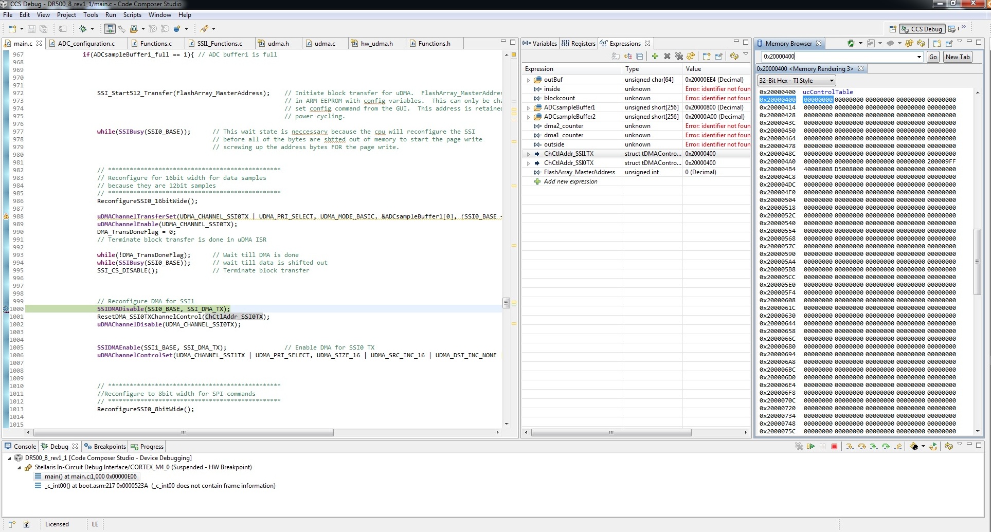
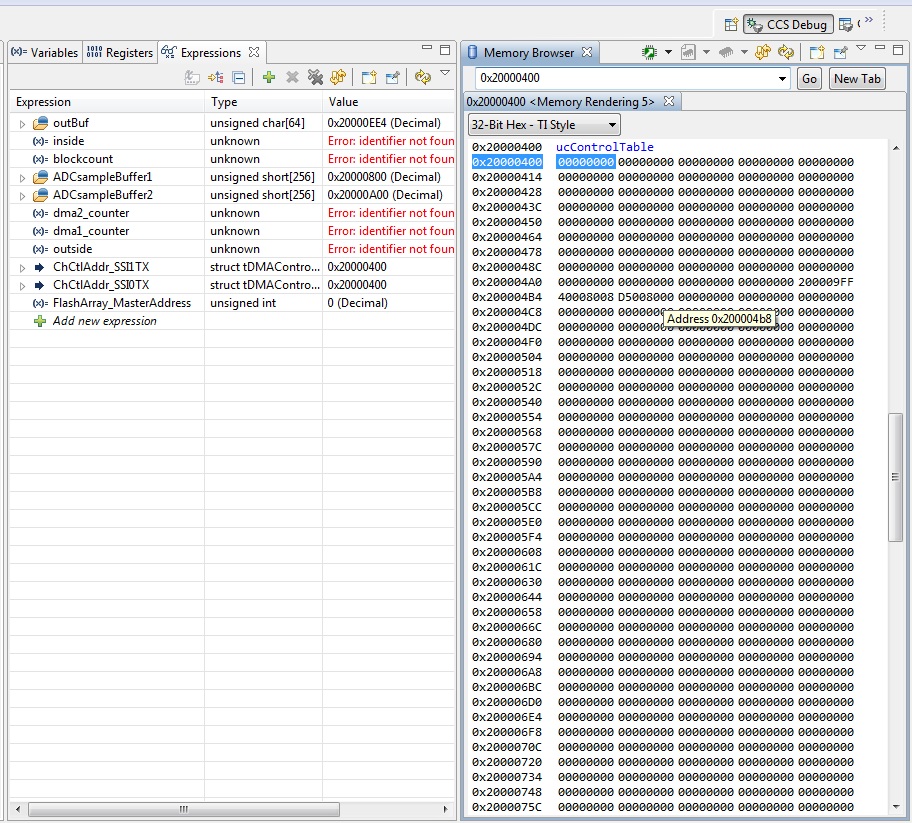
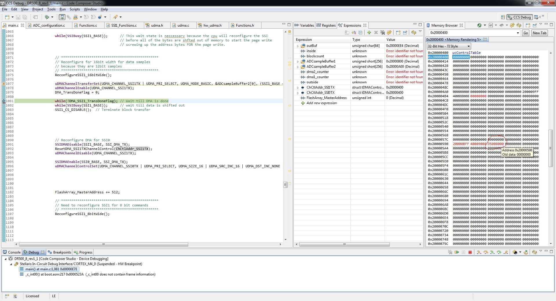
I'm using SSI0 and SSI1 to send data out.  I am triggering the DMA to send out blocks of data alternating between the two.  I'm unable to use SSI2 or SSI3 in this design.  I send out a lot of blocks of data between the two SSI ports so they alternate back and forth thousands of times.  After pushing a block out of SSI0 I then push a block out of SSI1 where BOTH SSI's are configured on their seperate DMA channels at all times.  I just trigger one channel then the other over and over.

It looks like (so far) that this is working fine.  I've gotten the board up and running pushing data out of both as described above and have tested this multiple times where it pushes blocks consisting of 0-256 and when I read the data back out it looks to be all correct. 

Potential problem:

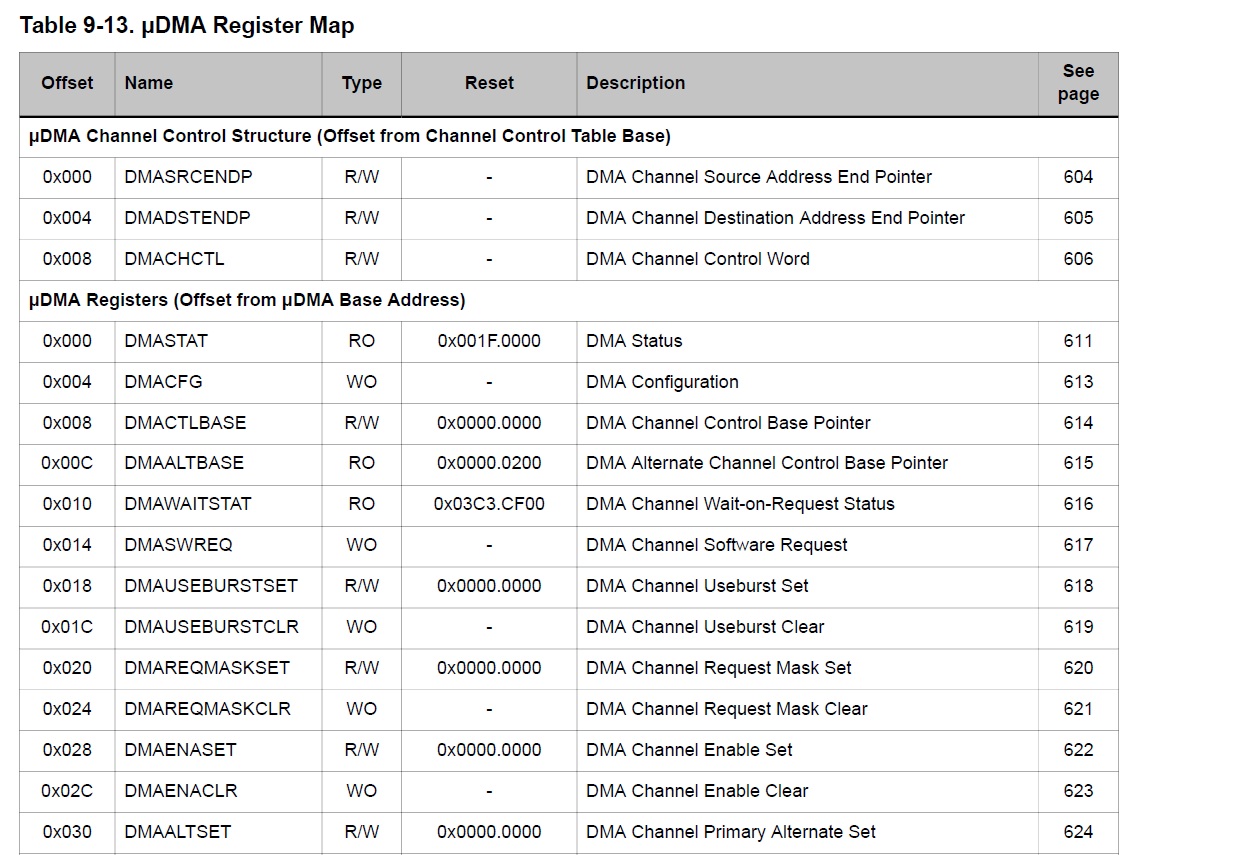
In reading the errata for this part I've found that for (per page 17) you can't use peripherals SSI0 and SSI1 on the uDMA.  It says "they cannot both be configured to use uDMA".  I don't want to move into production if I'm violating the errata, but I'm seeing no issues testing it here on the bench.  How do I know if this applies to me?  I can't find much info on my revision to know if it is revision 6 and 7?  I'm just looking for guidance because I don't want issues to pop up further down the road, but if I don't have to apply the work around (reconfiguring the DMA on the fly) it would save a lot of headache as this chip is pushed pretty hard as is.

Thanks,

Rob

  • Hello Rob,

    If the two SSI's are not being used at the same time for uDMA it should be OK. The problem will arise when the two SSI's are going to work concurrently for uDMA. Also do ensure that uDMA Channel is disabled for the SSI which is not being used.

    Regards

    Amit

  • Hey Amit,

    Thanks so much for your time!  My understanding is I need to adhere to this errata.  With that said, here is how I'm going about implementing the work around:

    My initial SSI/DMA configurations:

    	// ------------------------------
    	// Configure SSI0 module
    	// ------------------------------
    	SysCtlPeripheralEnable(SYSCTL_PERIPH_GPIOA);		// Enable SSI Port
    	GPIOPinConfigure(GPIO_PA2_SSI0CLK);					// Enable CLK pin
    	GPIOPinConfigure(GPIO_PA5_SSI0TX);					// Enable TX pin
    	GPIOPinConfigure(GPIO_PA4_SSI0RX);					// Enable RX pin
    	GPIOPinTypeSSI(GPIO_PORTA_BASE, GPIO_PIN_5 | GPIO_PIN_4 | GPIO_PIN_2);		// Enable comm. pins for SSI module
    	SysCtlPeripheralEnable(SYSCTL_PERIPH_SSI0);									// Enable SSI0 peripheral
    	SSIConfigSetExpClk(SSI0_BASE, SysCtlClockGet(), SSI_FRF_MOTO_MODE_0, SSI_MODE_MASTER, 20000000, 8);		// Configure SSI0 clk, buss speed, bit length, polarity/phase = 0/0, set as master
    	SSIEnable(SSI0_BASE);								// Enalbe SSI0
    
    	// enable uDMA for SSI
    	SSIDMAEnable(SSI0_BASE, SSI_DMA_TX);				// Enable DMA for SSI0 TX
    	IntEnable(INT_SSI0);								// Enable interrupt for SSI (this is actually over ridden by the uDMA meaning when the entire DMA (512 byte) DMA tx is done the int. is triggered)
    	uDMAChannelControlSet(UDMA_CHANNEL_SSI0TX | UDMA_PRI_SELECT, UDMA_SIZE_16 | UDMA_SRC_INC_16 | UDMA_DST_INC_NONE | UDMA_ARB_4);		// Configure channel control
    
    	// Enalbe CS pin for manual control
    	GPIOPinTypeGPIOOutput(GPIO_PORTA_BASE, GPIO_PIN_3);		// Set PA3 as CS pin for SSI which is toggled manually
    	GPIOPinWrite(GPIO_PORTA_BASE, GPIO_PIN_3, 0x08);		// Initialize to a high - no bus activity
    
    	// Empty SSI receive buffer
    	uint32_t emptySSI;		// dummy integer
        while(SSIDataGetNonBlocking(SSI0_BASE, &emptySSI))
        {	// loop to empty bus
        }	// non-blocking
        IntPrioritySet(INT_SSI0,  0x40);	// Lower interrupt priority


    	// ------------------------------
    	// Configure SSI1 module
    	// ------------------------------
        HWREG(GPIO_PORTF_BASE+GPIO_O_LOCK) = GPIO_LOCK_KEY;
        HWREG(GPIO_PORTF_BASE+GPIO_O_CR) = GPIO_PIN_0;
    
        GPIOPinConfigure(GPIO_PF0_SSI1RX);
        GPIOPinConfigure(GPIO_PF1_SSI1TX);
        GPIOPinConfigure(GPIO_PF2_SSI1CLK);
        GPIOPinTypeSSI(GPIO_PORTF_BASE, GPIO_PIN_0 | GPIO_PIN_1 | GPIO_PIN_2);
        SysCtlPeripheralEnable(SYSCTL_PERIPH_SSI1);
        SSIConfigSetExpClk(SSI1_BASE, SysCtlClockGet(), SSI_FRF_MOTO_MODE_0, SSI_MODE_MASTER, 20000000, 8);
        SSIEnable(SSI1_BASE);
    
    	// enable uDMA for SSI
    	//SSIDMAEnable(SSI1_BASE, SSI_DMA_TX);				// Enable DMA for SSI0 TX
    	IntEnable(INT_SSI1);								// Enable interrupt for SSI (this is actually over ridden by the uDMA meaning when the entire DMA (512 byte) DMA tx is done the int. is triggered)
    	uDMAChannelControlSet(UDMA_CHANNEL_SSI1TX | UDMA_PRI_SELECT, UDMA_SIZE_16 | UDMA_SRC_INC_16 | UDMA_DST_INC_NONE | UDMA_ARB_4);		// Configure channel control
    
    	// Enalbe CS pin for manual control
    	SysCtlPeripheralEnable(SYSCTL_PERIPH_GPIOC);
    	GPIOPinTypeGPIOOutput(GPIO_PORTC_BASE, GPIO_PIN_4);		// Set PC4 as CS pin for SSI1 which is toggled manually
    	GPIOPinWrite(GPIO_PORTC_BASE, GPIO_PIN_4, 0x10);		// Initialize to a high - no bus activity
    
    	// Empty SSI receive buffer
        while(SSIDataGetNonBlocking(SSI1_BASE, &emptySSI))
        {	// loop to empty bus
        }	// non-blocking
        IntPrioritySet(INT_SSI1,  0x40);	// Lower interrupt priority

    As you can see I basically configure these two the same, but without enabling DMA for SSI1.  Is this what TI means when they say they cannot be enabled/configured at the same time?  Basically, does this follow the intent of the work around?

    If so, I reconfigure these on the fly.  Is this satisfactory in meeting the requirement regarding only having one "Enabled" at a time.

    					SSIDMADisable(SSI0_BASE, SSI_DMA_TX);
    					SSIDMAEnable(SSI1_BASE, SSI_DMA_TX);
    
    					SSIDMADisable(SSI1_BASE, SSI_DMA_TX);
    					SSIDMAEnable(SSI0_BASE, SSI_DMA_TX);


    They are never enabled at the same time, but the part that i'm interested in here is that the channels ARE configured.  Said differently, I use the

    uDMAChannelControlSet(UDMA_CHANNEL_SSI1TX | UDMA_PRI_SELECT, UDMA_SIZE_16 | UDMA_SRC_INC_16 | UDMA_DST_INC_NONE | UDMA_ARB_4);

    call to configure the channel.  I'm unclear as to whether this violates the errata as well.  Any advice/insights here is greatly appreciated.

    Thanks,

    Rob

  • Hello Rob

    The condition as mentioned in the code is sufficient to ensure that DMA Request does not get asserted from the inactive SSI

    Regards

    Amit

  • Hey Amit,


    So I've been having problems getting reliable results out of my memory chips that are attached to these two spi ports (chip1 -> SSI0, chip2 -> SSI1).  I thought the errata was covered by the code above, but after a couple days of working on this I'm thinking we might have been wrong.  If I disable the DMA for SSI0 SSI1 pushes data into memory and when I read it back out (it's just a 16bit counter and I read out 65536 bytes) everything comes out fine.  If I used the above code (the one we thought was sufficient) I get intermittent blocks that are supposed to have gotten dma'd out dropping.  Some of the data blocks dma'd into memory are just not there when I read the 65536 bytes out.  It is not the same blocks if I run multiple iterations....said differently, the dma blocks of data that get dropped change.  

    My debug setup is like this:

    I basically completely disable one SSI's DMA and try to get the other to run correctly.  I then swap them and repeat with the opposite SSI DMA channels.  I'm just using one SSI at a time to pin point this issue.  I've gotten them to run correctly one at a time now, but I've had 0 success in getting a work-around to work for this eratta problem.

    One question I have is what is the difference between these to API calls?

    					SSIDMADisable(SSI0_BASE, SSI_DMA_TX);
    					uDMAChannelDisable(UDMA_CHANNEL_SSI0TX);

      I've tried replacing the above enable/disable blocks with this and still no luck.

    					// Reconfigure DMA for SSI1
    					SSIDMADisable(SSI0_BASE, SSI_DMA_TX);
    					uDMAChannelDisable(UDMA_CHANNEL_SSI0TX);
    					uDMAChannelEnable(UDMA_CHANNEL_SSI1TX);
    					SSIDMAEnable(SSI1_BASE, SSI_DMA_TX);

    I'm running out of ides to try to get around this eratta problem.  I noticed that the eratta says the channel can't be configured either.  Does that mean this call:

    uDMAChannelControlSet(UDMA_CHANNEL_SSI0TX | UDMA_PRI_SELECT, UDMA_SIZE_16 | UDMA_SRC_INC_16 | UDMA_DST_INC_NONE | UDMA_ARB_4);

    needs to be undone or disabled as well as the channel?  I'm not missing a lot of dma data blocks, it is usually less than 10, but this is a really big problem for me.  I'm unable to use the SSI2 or SSI3 because of other peripheral and hardware requirements.  I guess what I'm looking for here is some more information regarding the first function calls I asked about and a response about how confident you are that all I need to do is what I posted above which really doesn't seem to work where the SSI's dma channels work as long as the other one isn't configured at all.  Said differently I've tried swapping between the two every way I could come up with and nothing is working.

    Note:

    I've just done some more test runs and the results show me that when I ONLY disable the

    SSIDMAEnable(SSI0_BASE, SSI_DMA_TX);

    call and run the other SSI it fails.  When I ALSO comment out this call:

    uDMAChannelControlSet(UDMA_CHANNEL_SSI0TX | UDMA_PRI_SELECT, UDMA_SIZE_16 | UDMA_SRC_INC_16 | UDMA_DST_INC_NONE | UDMA_ARB_4);

    it runs correctly and consistently.  It's looking like the crux is both but I don't know how to "un-configure" the ChannelControlSet call.

    Thanks,

    Rob

  • Hello Robbie,

    Yes, the uDMAChannelControlSet call has to be removed. Another way to do so (since there is no unset) is to read the UDMA_CTLBASE address and then add (0x10*11)+0x08 to get the Control Word Entry and make it 0x0.

    Regards

    Amit

  • Could you elaborate on how to read the UDMA_CTLBASE (it doesn't seemed to be defined in my project) and where you got the (0x10*11)+0x08?  Is that from the DMA control table?

    I see in the datasheet it says that the dma register addresses given are relative to the dma base address of 0x400F.F000.  Is that the UDMA_CTLBASE address?  I'm a little confused because 0x10 * 11 is (0x10)(0x0B) is 0xB0 which I can't find that address in the data sheet dma registers section.  In looking at this register 20 is 0x04C and then it jumps to 0x500.

    I'm assuming the 0x08 comes from the data sheet in the pic below:

    My control table looks like this:

    //*****************************************************************************
    //
    // The control table used by the uDMA controller.  This table must be aligned
    // to a 1024 byte boundary.
    //
    //*****************************************************************************
    #if defined(ewarm)
    #pragma data_alignment=1024
    unsigned char ucControlTable[1024];
    #elif defined(ccs)
    #pragma DATA_ALIGN(ucControlTable, 1024)
    unsigned char ucControlTable[1024];
    #else
    unsigned char ucControlTable[1024] __attribute__ ((aligned(1024)));
    #endif

    but I'm not sure how I find the address of that 1024 byte table and then modify it.

    ** Also do i need to use this call as well?

    uDMAChannelDisable(UDMA_CHANNEL_SSI1TX);

  • Hello Robbie,

    It is the register at offset 0x008 (UDMACTLBASE) and is defined in the hw_udma.h

    The equation is from the DMA Control Base Table and can be used to access the same in the SRAM ina generic form as

    Source Address Pointer = (0x10*N)

    Destination Address Pointer = (0x10*N) + 0x004

    Control Word Address Pointer = (0x10*N) + 0x008

    where N is the channel on which the DMA Request is Mapped (0-31 are the valud values).

    Also do keep the channel disabled.

    Regards

    Amit

  • Hey Amit,


    I had to spend last night and today studying up on the DMA but now I understand.  I'll show you what I am doing to see what you think because I'm still not having any luck. 

    After I send out a block of data to memory over DMA SSI0 I run this code to switch over to SSI1 DMA:

    					// Reconfigure DMA for SSI1
    					SSIDMADisable(SSI0_BASE, SSI_DMA_TX);
    					ResetDMA_SSI0TXChannelControl(ChCtlAddr_SSI0TX);
    					uDMAChannelDisable(UDMA_CHANNEL_SSI0TX);
    
    
    					SSIDMAEnable(SSI1_BASE, SSI_DMA_TX);				// Enable DMA for SSI0 TX
    					uDMAChannelControlSet(UDMA_CHANNEL_SSI1TX | UDMA_PRI_SELECT, UDMA_SIZE_16 | UDMA_SRC_INC_16 | UDMA_DST_INC_NONE | UDMA_ARB_4);

    The function:

    ResetDMA_SSI0TXChannelControl(ChCtlAddr_SSI0TX);

    is this:

    void ResetDMA_SSI0TXChannelControl(tDMAControlTable * base){
    
    	tDMAControlTable *psCtl;
    
    
        //
        // Get the base address of the control table.
        //
        psCtl = base;
    
    
        // Clear UDMACHCTL word in table
        //psCtl[(0x10*11)+0x08].ui32Control = 0x00;
        psCtl[(11)].ui32Control = 0x00;
    
    
    }

    and I am passing it this:

    tDMAControlTable *ChCtlAddr_SSI0TX;
    tDMAControlTable *ChCtlAddr_SSI1TX;
    
    ChCtlAddr_SSI0TX = 0;
    ChCtlAddr_SSI1TX = 0;
    
    
    	//
    	// Configure DMA for SSI
    	//
    	SysCtlPeripheralEnable(SYSCTL_PERIPH_UDMA);
    	uDMAEnable();
    	uDMAControlBaseSet(ucControlTable);


    	ChCtlAddr_SSI0TX = (tDMAControlTable *)HWREG(UDMA_CTLBASE);		// ****** DEBUG *********
    	ChCtlAddr_SSI1TX = (tDMAControlTable *)HWREG(UDMA_CTLBASE);

    Just so you can see where that variable is coming from.  The "ChCtlAddr_SSI0TX" variable is the address of the DMA control table.  I can verify this below:

    In the expressions window you can see the two variables ChCtlAddr_ssI1 and SSI0TX that hold the value 0x20000400 which is the the address of the dma control table.  In the memory browser you can see that that address really is the ucControlTable as described in my code like this:

    //*****************************************************************************
    //
    // The control table used by the uDMA controller.  This table must be aligned
    // to a 1024 byte boundary.
    //
    //*****************************************************************************
    #if defined(ewarm)
    #pragma data_alignment=1024
    unsigned char ucControlTable[1024];
    #elif defined(ccs)
    #pragma DATA_ALIGN(ucControlTable, 1024)
    unsigned char ucControlTable[1024];
    #else
    unsigned char ucControlTable[1024] __attribute__ ((aligned(1024)));
    #endif
    

    Now the address we talked about above is the 11'th row basically which is a structure defined in the UDMA.c file and looks like this.

    //*****************************************************************************
    //
    // A structure that defines an entry in the channel control table.  These
    // fields are used by the uDMA controller and normally it is not necessary for
    // software to directly read or write fields in the table.
    //
    //*****************************************************************************
    typedef struct
    {
        //
        // The ending source address of the data transfer.
        //
        volatile void *pvSrcEndAddr;
    
        //
        // The ending destination address of the data transfer.
        //
        volatile void *pvDstEndAddr;
    
        //
        // The channel control mode.
        //
        volatile uint32_t ui32Control;
    
        //
        // An unused location.
        //
        volatile uint32_t ui32Spare;
    }
    tDMAControlTable;

    So what I did was get the address of that table and pass it to my function that resets the channel control word (function shown above).

    This instruction:

    psCtl[(11)].ui32Control = 0x00;

    in that function erases that word.  psCtl holds the address of the table and I then move down 11 times (or move down 11 of the tDMAControlTable structures) to get to the one for SSI0 and use dot notation to clear word 0x08.  I am confident this is what you recommended above.  Using your numbers I get a memory address of B8 for the channel control word I need to clear because (0x10*11) + 0x08 = (16*11) + 8 = 184 in decimal.  This would be the offset from my control table address.  Adding these two together I get a total memory address for the dma channel control word I need to clear as 0x200004b8.  Below are the values loaded in memory for this address in the control table just to verify.

    My cursor is hovering over the word D5008000 which is the above mentioned memory address.  So, at this point it looks like the channel is configured correctly.  If you run those same calculations for SSI1_TX (which is 0x10*25)+0x08 away you get an address of 0x20000598 which is zero in the above pic so that channel is completely zero'd out.  Now after reconfiguring with my reconfigure function that clears the SSI0_TX control word and configures the SSI1_TX control word I get this:

    I've circled the address in red, but as you can see with the mouse hovering over 0xD5008000 I get the correct memory address using the calculations of (0x10*25)+0x08 as I used the first time just applied to SSI1_TX this time.  Now If I run to the first break point again where they are supposed to swap back I get this:

    I've again circled the two respective control table channel address words that I'm supposed to be clearing and reconfiguring and it looks like this is working fine.  The entire word is cleared and reconfigured. 

    Unfortunately this work-around still is not working though.  As before if I run 1 channel at a time my data is consistent and none of the blocks pushed out by the DMA get dropped.  If I added in the second SSI/DMA it goes right back to dropping blocks of data that the dma is supposed to be pushing out and it is not always the same amount of blocks.  I am fairly confident this is the eratta problem because any data that is dropped is ALWAYS dropped in 512 byte blocks which is what the DMA is supposed to be moving.  I'm also confident I'm clearing the correct data in the control table because the channel control words are the same and that makes sense because the channel control set function configures them exactly the same parameter wise. 


    This is more of a status update to show you the results of our last few posts.  It was a great idea and I know understand how the DMA works much better lol but I'm still stuck.  I don't have a particular question at the moment as I'm still modding/debugging and running the code to try to glean more insight out of this, but I wanted to get you these results fairly quickly in case you had some other ideas.


    One note:

    I put a counter in front of the call to enable the dma channel to push data and one counter in the SSI1 ISR that gets called every time the block of data is pushed out.  Both of these counters line up every time.  I was wondering if this is strange.  It seems like if they both line up the dma thinks it is working because the interrupt from it finishing is getting triggered reliably.  I'm not sure if this information could prove that I'm just missing something somewhere else and maybe it isn't the errata problem....I'm not sure what to make of this.

    Another note (just to be thorough):

    In this firmware I am changing up the serial port so I figured I'd post this code quick just in case the problem is not in the errata anymore.  The code that moves the data to memory goes like this.  Send out 8bit commands to open up page write for memory chip, change SSIx over to 16bit width to dump two bytes of data at a time (512 bytes total over 256 iterations of the dma loading the SSIx_TX buffer) reconfigure SSI back to 8 bit width for the next set of page write commands when I come back around to sending out another via this SSI port.  This code is run during all of this other reconfiguring so I figured I'd post it up in case it is helpful.

    I send the page write commands, block while they are being sent out then reconfigure the SSIx port to 16bit width using this code:

    void ReconfigureSSI1_16bitWide()
    {
    	//
    	// Configure SSI module
    	//
    	SSIDisable(SSI1_BASE);								// Disable SSI0
    
    	SSIConfigSetExpClk(SSI1_BASE, SysCtlClockGet(), SSI_FRF_MOTO_MODE_0, SSI_MODE_MASTER, 20000000, 16);		
    	SSIEnable(SSI1_BASE);								
    
    	// enable uDMA for SSI
    	SSIDMAEnable(SSI1_BASE, SSI_DMA_TX);				// Enable DMA for SSI0 TX
    	IntEnable(INT_SSI1);								
    
    
        IntPrioritySet(INT_SSI1,  0x40);	// Lower interrupt priority
    }

    I then kick off the DMA and block until both the DMA is done (throws it's interrupt saying all 512 bytes are done being moved) and block until the SSIx is done shifting out all data. I do this with while loops.  I then end the page writing by driving chip select low and reconfigure back to 8 bit width with this code.

    SSIDisable(SSI1_BASE);
    SSIConfigSetExpClk(SSI1_BASE, SysCtlClockGet(), SSI_FRF_MOTO_MODE_0, SSI_MODE_MASTER, 20000000, 8);
    SSIEnable(SSI1_BASE);	
    IntEnable(INT_SSI1);
    IntPrioritySet(INT_SSI1,  0x40);

    After this I run the code we've been discussing.  Just some more info.


    Thanks,

    Rob

  • Hey Amit,

    I finally got this working.  The work around described in your post does work now.  I was incorporating it into a larger ccs project and for some reason it was just very difficult.  I ended up going in circles for a long time because initially I couldn't get that work around to work in the obvious straight forward manner as discussed.  I'm not exactly sure what all the problems were, but I am suspect of the tiva launchpad as a programmer/debugger which is what I've been using.  Sometimes I will be developing and things just don't seem to be acting right and I think something strange was going on between that launchpad and my custom board and USB. 

    Anyways, I will try to post up some solution code to the workaround for others and Amits guidance does seem to work.  I've tested this fairly well and all of my data is now spot on thus far and I'm moving ~1M bytes over these to SSI peripherals so I feel pretty good about that.  As usual these forums and the ppl on here have helped me out greatly!

    Thanks again Amit!  I'll put up some of my code regarding clearing the dma control table channel data soon as well.

    Thanks,

    Rob

  • Hello Rob,

    Yes, indeed a code post would be good for a lot of folks in the community. Also I would take this back to the errata so that the document does a better job too.

    Apologies for not having responded earlier.

    Regards

    Amit

  • Hi Rob,

    I would be interested to see any code snippets you could share.

  • Hey sorry for the late reply.  Here is what I'm doing for a work around.

    					// Reconfigure DMA for SSI1
    					SSIDMADisable(SSI0_BASE, SSI_DMA_TX);
    					ResetDMA_SSI0TXChannelControl(ChCtlAddr_SSI0TX);

    That function is defined as:

    void ResetDMA_SSI0TXChannelControl(tDMAControlTable * base){
    
    	tDMAControlTable *psCtl;
    
    
        //
        // Get the base address of the control table.
        //
        psCtl = base;
    
    
        // Clear UDMACHCTL word in table
        //psCtl[(0x10*11)+0x08].ui32Control = 0x00;
        psCtl[(11)].ui32Control = 0x00;
    
    
    }

    After executing the above code I then configure SSI1

    					SSIDMAEnable(SSI1_BASE, SSI_DMA_TX);				// Enable DMA for SSI0 TX
    					uDMAChannelControlSet(UDMA_CHANNEL_SSI1TX | UDMA_PRI_SELECT, UDMA_SIZE_16 | UDMA_SRC_INC_16 | UDMA_DST_INC_NONE | UDMA_ARB_4);

    That configures SSI1 Channel.  When I break into the state where I send out data over SSI1 I send data then reconfigure back to SSI0:

    					// Reconfigure DMA for SSI0
    					SSIDMADisable(SSI1_BASE, SSI_DMA_TX);
    					ResetDMA_SSI1TXChannelControl(ChCtlAddr_SSI1TX);
    
    
    					SSIDMAEnable(SSI0_BASE, SSI_DMA_TX);
    					uDMAChannelControlSet(UDMA_CHANNEL_SSI0TX | UDMA_PRI_SELECT, UDMA_SIZE_16 | UDMA_SRC_INC_16 | UDMA_DST_INC_NONE | UDMA_ARB_4);

    Basically the same function to clear the channel control set table.

    void ResetDMA_SSI1TXChannelControl(tDMAControlTable *base){
    
    	tDMAControlTable *psCtl;
    
    
        //
        // Get the base address of the control table.
        //
        psCtl = base;
    
    
        // Clear UDMACHCTL word in table
        //psCtl[(0x10*25)+0x08].ui32Control = 0x00;
        psCtl[(25)].ui32Control = 0x00;
    
    
    }

    The big difficulty for me was figuring out that this simple code would work.  In a complex system not knowing exactly what to do makes it difficult to debug run time errors which is what was killing me.  One big key for me was spending time to understand the channel control table.  Understand it!  It makes things easier.  Also understand that this:

    uDMAControlBaseSet(ucControlTable);

    Sets the address of the table into a point basically (I think but I'm not a pro here so someone correct me if I'm wrong), but it just loads the address of the table into another memory address.  This is very handy because you can access the register that this function call stores the table address in to GET the address of the table and store it in a pointer.  After this check out the typdef that defines the table...

    typedef struct
    {
        //
        // The ending source address of the data transfer.
        //
        volatile void *pvSrcEndAddr;
    
        //
        // The ending destination address of the data transfer.
        //
        volatile void *pvDstEndAddr;
    
        //
        // The channel control mode.
        //
        volatile uint32_t ui32Control;
    
        //
        // An unused location.
        //
        volatile uint32_t ui32Spare;
    }
    tDMAControlTable;

    This defines a table entry.  If you do what I did you can grab the address of the table, stick it in a pointer and use that structure to access the elements in each row basically.  For reference check out what TI does to load data into a table channel row.

    11 and 25 are the address offsets in the table for SSI0_TX channel and SSI1_TX channel.

    void
    uDMAChannelControlSet(uint32_t ui32ChannelStructIndex, uint32_t ui32Control)
    {
        tDMAControlTable *psCtl;
    
        //
        // Check the arguments.
        //
        ASSERT((ui32ChannelStructIndex & 0xffff) < 64);
        ASSERT(HWREG(UDMA_CTLBASE) != 0);
    
        //
        // In case a channel selector macro (like UDMA_CH0_USB0EP1RX) was
        // passed as the ui32ChannelStructIndex parameter, extract just the channel
        // index from this parameter.
        //
        ui32ChannelStructIndex &= 0x3f;
    
        //
        // Get the base address of the control table.
        //
        psCtl = (tDMAControlTable *)HWREG(UDMA_CTLBASE);
    
        //
        // Get the current control word value and mask off the fields to be
        // changed, then OR in the new settings.
        //
        psCtl[ui32ChannelStructIndex].ui32Control =
            ((psCtl[ui32ChannelStructIndex].ui32Control &
              ~(UDMA_CHCTL_DSTINC_M |
                UDMA_CHCTL_DSTSIZE_M |
                UDMA_CHCTL_SRCINC_M |
                UDMA_CHCTL_SRCSIZE_M |
                UDMA_CHCTL_ARBSIZE_M |
                UDMA_CHCTL_NXTUSEBURST)) |
             ui32Control);
    }


    It looks complicated, but if you unpack it it isn't too bad.  This is effectively what I did, but backwards.  They store the address from one of the first functions I listed that saves the address of the table and they just stick that address in a pointer and typcast it to that typdef above.  After that it's just like an array basically where the channel structIndex value is the channel offset discussed in above posts and the control is the control data you have to clear and set for the workaround. 


    I have more testing to do, but so far my data moving in and out of SSI0 and SSI1 looks good and I'm currently held up by some non-embedded design stuff so if I have a problem I'll report back and if not I would assume this is the fix implemented for the TivaC part I'm using.


    Let me know if you have any questions or anything....it was a tough problem to solve, but taking it step by step is key and Amit's advices seemed to be on point.

  • Hello Robbie,

    Thanks for the code. I would take this as a feedback for the errata to be updated as well to make user life simpler.

    Regards

    Amit

  • Awesome!  Yea, I'll say as a customer it is frustrating because there are so many smart people that understand this at ti I get annoyed that they can't just write it out in code even as an example.  I know there are example programs, but I feel like after going through this it would be so easy for TI to do it doesn't make sense to have customers re-inventing the wheel so to speak.  You guys do a lot of things right too though so I'm not hating...this form is really an outstanding resource and puts some other companies forums to shame like Altera.