This thread has been locked.

If you have a related question, please click the "Ask a related question" button in the top right corner. The newly created question will be automatically linked to this question.

Synchronizing two SPI channels via uDMA?

Dear community,

i am using the TM4C1231 Tiva part, and i'm faced with a tricky situation for that i'm hoping for some of your advise. I am working with a PWM LED driver part, that uses a serial SPI-like communication scheme to transmit the PWM/grayscale data to it. However, this part seems to be designed to be used rather with programmable hardware than with a microcontroller.

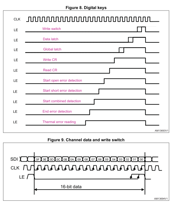
In it's comminication scheme, 16-bit data is transmitted synchronously over two wires, CLK and DATA in a SSI/SPI fashion. However, a third control line is used to signal commands to the driver IC, such as latching data, enabling/disabling outputs and more. This control line is also synchronized to the CLK signal, and the number of CLK pulses it goes high after determines the command. (For more information feel free to look at the LED1642 datasheet).

My only solution so far to support this synchronous transmission scheme is to use soft-SPI plus the control line, which has the two obvious downsides: 1. The speed is low, 2. The CPU is constantly busy transmitting display data.

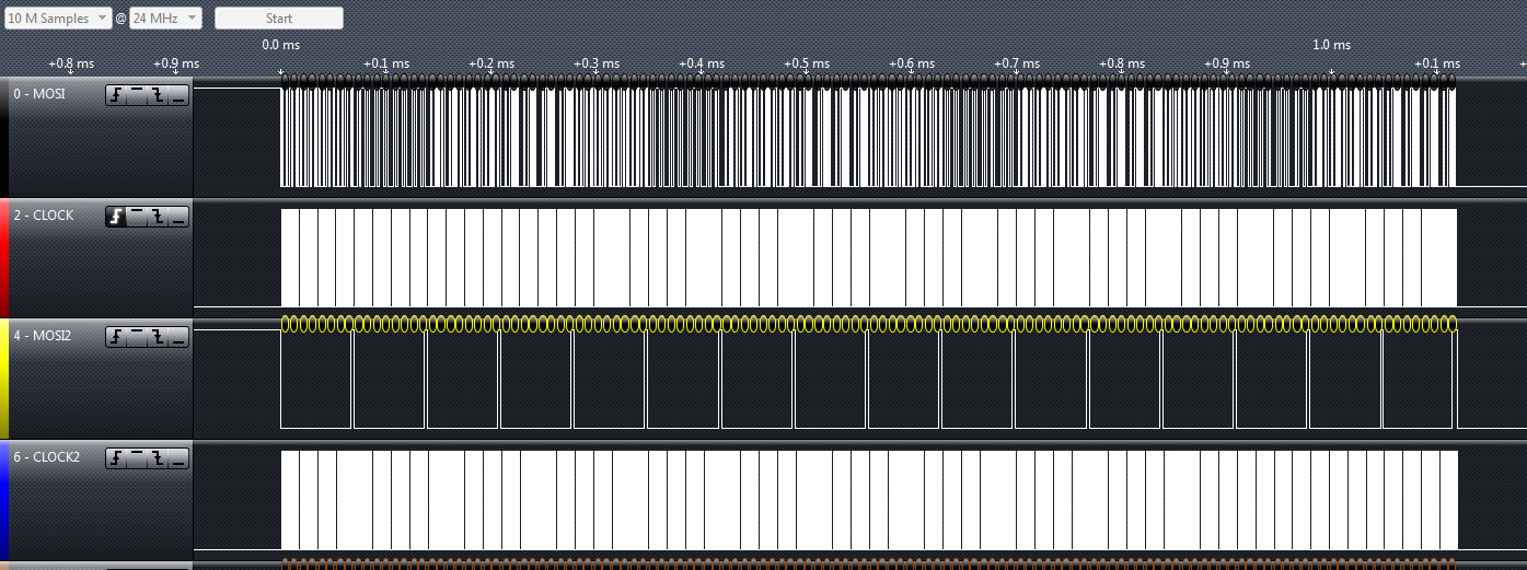
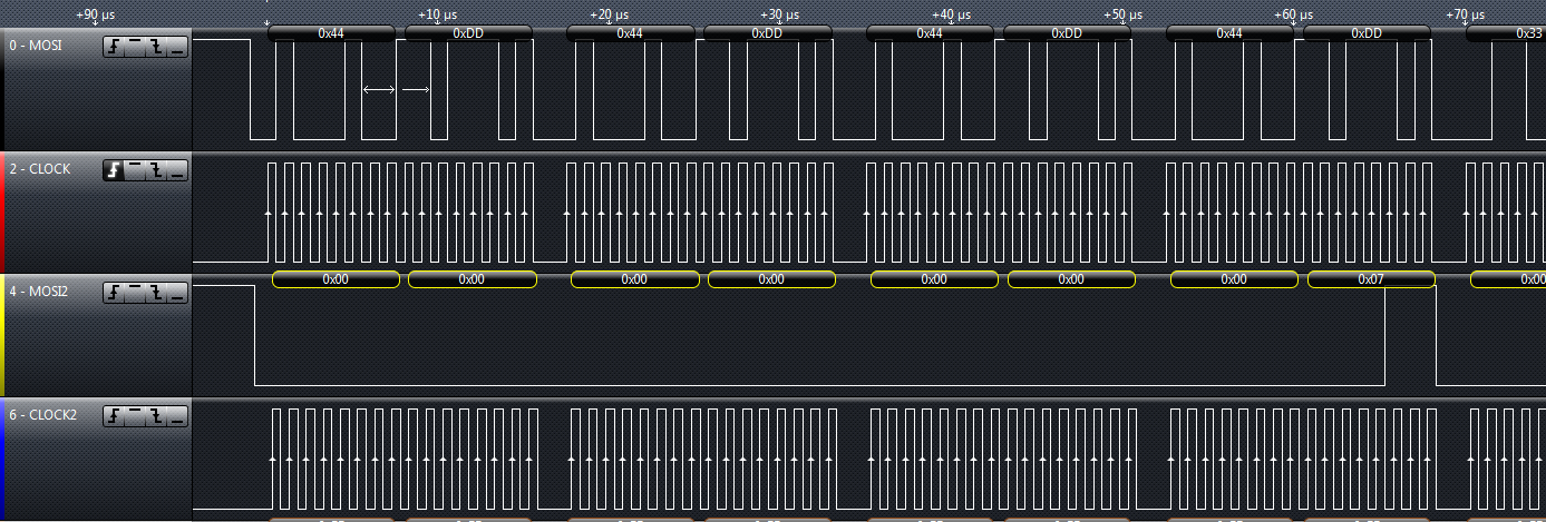
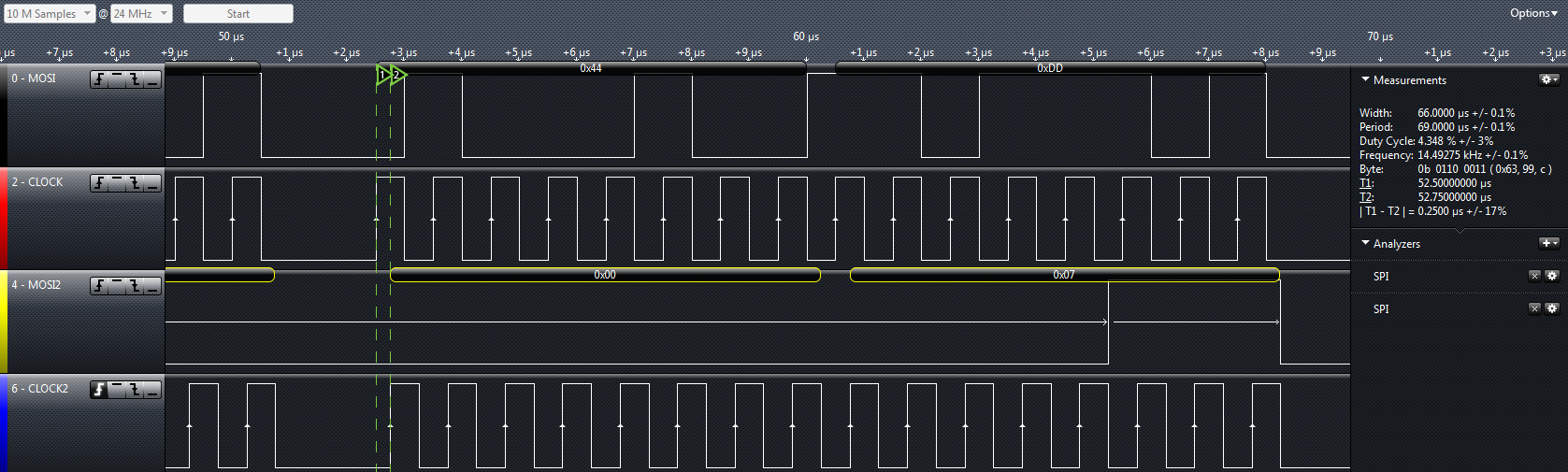
Initially I was hoping to get the serial communication to be performed by the uDMA module in the background, but even using SPI without uDMA doesn't work because of the control line scheme of the driver IC. So i was hoping to synchronize two SPI channels together using uDMA, using two buffers, the one containing the actual PWM/grayscale data, transferred over SSI0/uDMA, and the other containing the corresponding control command data, transferred over SSI2/uDMA. However i already noticed, that the SSI transmissions don't start synchronously, there seems to be a gap of around 1 clock cycle between the starts. (Unfortunately, i don't have precise measurement equipment - a 24MHz logic analyzer is all i have, yet).

So having the uDMA controller synchronize the transmissions doesn't seem to work, unless i would have a guaranteed delay between the starts of the SSI transmission. (In this case, i could calculate the shifts into my control-line-buffer). But i doubt that there is a guarantee that can be made.

Is there anything else i can to to synchronize this third control line into the SPI transmission, that is performed via uDMA? Can you guys think of anything, except having to find another PWM driver and re-design?

Appending also the code that i'm using to try out the parallel SSI transmission.

Thanks,

Janos

#include <stdbool.h>
#include <stdint.h>

#include "inc/hw_types.h"
#include "inc/hw_ints.h"
#include "inc/hw_ssi.h"
#include "inc/hw_udma.h"
#include "driverlib/pin_map.h"
#include "driverlib/interrupt.h"
#include "driverlib/sysctl.h"
#include "driverlib/udma.h"
#include "driverlib/gpio.h"
#include "driverlib/ssi.h"

#define MEM_BUFFER_SIZE         16

uint8_t ui8ControlTable[1024] __attribute__ ((aligned(1024)));

static uint8_t bufferSSI0[MEM_BUFFER_SIZE];
static uint8_t bufferSSI2[MEM_BUFFER_SIZE];

#define SPI_CLK_SPEED_Hz 12000000

void SSI0_Init(void) {
	SysCtlPeripheralEnable(PERIPH(SSI0));
	SysCtlPeripheralEnable(PERIPH_GPIO(A));
	GPIOPinConfigure(GPIO_PA2_SSI0CLK);
	GPIOPinConfigure(GPIO_PA5_SSI0TX);
	GPIOPinTypeSSI(PORT(A), PIN(5) | PIN(2));
	SSIConfigSetExpClk(SSI0_BASE, SysCtlClockGet(), SSI_FRF_MOTO_MODE_0, SSI_MODE_MASTER, SPI_CLK_SPEED_Hz, 8);
	SSIEnable(SSI0_BASE);
	uint32_t tmp;
	while (SSIDataGetNonBlocking(SSI0_BASE, &tmp)) {
	}
}

void SSI2_Init(void) {
	SysCtlPeripheralEnable(PERIPH(SSI2));
	SysCtlPeripheralEnable(PERIPH_GPIO(B));
	GPIOPinConfigure(GPIO_PB4_SSI2CLK);
	GPIOPinConfigure(GPIO_PB7_SSI2TX);
	GPIOPinTypeSSI(PORT(B), PIN(7) | PIN(4));
	SSIConfigSetExpClk(SSI2_BASE, SysCtlClockGet(), SSI_FRF_MOTO_MODE_0, SSI_MODE_MASTER, SPI_CLK_SPEED_Hz, 8);
	SSIEnable(SSI2_BASE);
	uint32_t tmp;
	while (SSIDataGetNonBlocking(SSI2_BASE, &tmp)) {
	}
}

void SSI0_uDMA_Enable(uint8_t *source, uint32_t len) {
    SSIDMAEnable(SSI0_BASE, SSI_DMA_TX);
    uDMAChannelAttributeDisable(UDMA_CHANNEL_SSI0TX,
                                    UDMA_ATTR_ALTSELECT |
                                    UDMA_ATTR_HIGH_PRIORITY |
                                    UDMA_ATTR_REQMASK);
    uDMAChannelAttributeEnable(UDMA_CHANNEL_SSI0TX, UDMA_ATTR_USEBURST);
    uDMAChannelControlSet(UDMA_CHANNEL_SSI0TX | UDMA_PRI_SELECT,
                              UDMA_SIZE_8 | UDMA_SRC_INC_8 | UDMA_DST_INC_NONE |
                              UDMA_ARB_4);
    uDMAChannelTransferSet(UDMA_CHANNEL_SSI0TX | UDMA_PRI_SELECT,
                               UDMA_MODE_BASIC,
                               source,
                               (void *)(SSI0_BASE + SSI_O_DR),
                               len);
}
void SSI2_uDMA_Enable(uint8_t *source, uint32_t len) {
    SSIDMAEnable(SSI2_BASE, SSI_DMA_TX);
    uDMAChannelAssign(UDMA_CH13_SSI2TX);
    uDMAChannelAttributeDisable(UDMA_CH13_SSI2TX,
                                    UDMA_ATTR_ALTSELECT |
                                    UDMA_ATTR_HIGH_PRIORITY |
                                    UDMA_ATTR_REQMASK);
    uDMAChannelAttributeEnable(UDMA_CH13_SSI2TX, UDMA_ATTR_USEBURST);
    uDMAChannelControlSet(UDMA_CH13_SSI2TX | UDMA_PRI_SELECT,
                              UDMA_SIZE_8 | UDMA_SRC_INC_8 | UDMA_DST_INC_NONE |
                              UDMA_ARB_4);
    uDMAChannelTransferSet(UDMA_CH13_SSI2TX | UDMA_PRI_SELECT,
                               UDMA_MODE_BASIC,
                               source,
                               (void *)(SSI2_BASE + SSI_O_DR),
                               len);
}

int main(void) {

	SysCtlClockSet(SYSCTL_SYSDIV_2_5 | SYSCTL_USE_PLL | SYSCTL_OSC_INT | SYSCTL_XTAL_16MHZ);

	unsigned int i;
	for (i = 0; i < MEM_BUFFER_SIZE; i++) {
		bufferSSI0[i] = i;
		bufferSSI2[i] = MEM_BUFFER_SIZE - i;
	}

	SysCtlPeripheralEnable(SYSCTL_PERIPH_UDMA);
	SysCtlPeripheralSleepEnable(SYSCTL_PERIPH_UDMA);
	uDMAEnable();
	uDMAControlBaseSet(ui8ControlTable);

	SysCtlPeripheralEnable(PERIPH_GPIO(A));
	GPIOPinTypeGPIOOutput(PORT(A), PIN(3));
	GPIOPinWrite(PORT(A), PIN(3), 0);

	SSI0_Init();
	SSI2_Init();

	SSI0_uDMA_Enable(bufferSSI0, MEM_BUFFER_SIZE);
	SSI2_uDMA_Enable(bufferSSI2, MEM_BUFFER_SIZE);

	uDMAChannelEnable(UDMA_CHANNEL_SSI0TX);
	uDMAChannelEnable(UDMA_CH13_SSI2TX);

	while (1) {
	}
}

  • Janos said:
    ... a third control line is used to signal commands to the driver IC, such as latching data, enabling/disabling outputs and more. This control line is also synchronized to the CLK signal, and the number of CLK pulses it goes high after determines the command.

    Commend you for a very well described - high effort post.  Makes your (vendor agnostic) remote staff  "want" to assist.  And just maybe - we can...

    Have been many moons in the display biz - designed/produced, "intelligent, 5x7 dot matrix Led modules prior to the introduction of the first, HD-44780 based Lcd modules.  So know my way around such scanned, multiplexed, control impementations - at least somewhat...

    Do note that I'm making no attempt to, "Sync 2 SPI channels under uDMA" - I'm after a faster/easier (i.e. KISS) method. (about all my limited brain allows)

    A great simplification can be had if that, "3rd control line" can, "arrive and set-up" - slightly prior to the sync clock. (from past experience I believe that flexibility is normal/customary.)  I believe that both your SDI data and the control line are read via the sync clock - but I don't believe that the control line must arrive in "sync" with that clock. And - I believe that "sync'ed arrival" is your belief - and unduly complicates.  (again - my experience is that the data and control bits (if any) are read in "one gulp" - but only after a (typical) 1/2 clock period delay.  (this is so as it makes the SIPO receiver far more immune to set-up/hold type of errors)  And that same 1/2 clock period (or opposite clock edge) is employed as part of the "normal" SPI scheme - as well.

    Should this prove the case - cannot you feed your SPI clock to an (unused) GPIO input (perhaps assign that bit to a fast GPIO Port) and then interrupt upon the # of SPI clocks equaling your desired control/command clock count? And then - have that interrupt service immediately generate a fast port GPIO output - which serves as the LE (i.e. control signal) in your diagram?  *** Indeed - that LE I've just manufactured is sync'ed to "no man" - but so long as it arrives prior to the next sync clock "read edge" - all should be well!  (one hopes!)

    Now for this to succeed I believe 2 things must land in our favor:

    a) that LE/control signal is not forced to arrive in exact sync w/the SPI clock  (1/2 clock delay - as described above - is tolerated

    b) your MCU's response to the, "SPI clock count" reaching target enables the generation of the GPIO output bit (serving as LE/control) in time to be correctly registered by the sync clock.  (i.e. generates & arrives ahead of the next sync clock "read."

    We may ease this somewhat (I'd recommend) by slowing the SPI clock during initial, "test - proof of concept."  As/if it works - you may gradually increase speed - always monitoring the BER (bit error rate) for signal fall-out.

    We've also used FPGAs (often to replace several boards worth of military logic) and can report that this MCU -massaged method has worked - has proved robust - although each case brings its own wrinkles - and must be individually examined.

    That's this reporter's opinion/counsel - bon chance mon ami...  

    And - we note that while you're relatively new here - already you've jumped in and have offered valuable guidance - to others.  That's great - very much the spirit of the forum - know that your efforts are welcome & appreciated...

  • Hi cb,

    thanks so much for your great idea and detailled suggestion! (I nearly missed it, as when i was looking earlier into it, i saw only a short note). I appreciate your appreciation of my activities - I am very new here indeed, and hoping that I can give some of the help and advise back to others. That's the least I can try to do, plus i get the bonus of learning much quicker when I try to figure out the trouble of others. Such as you guys do, and let me say this, i am still new here but i already got to like to look into your posts and comments, when i see them. It's always good and well thought advise.

    So back to it... I like your approach very much, and i have tried to take it a little bit further. You are perfectly right with your assumption/hope concerning the "sync" of the control signal against the CLK signal. The datasheet doesn't make it very clear, but from my attempts it seems that the control line just has to be high, when the CLK signal goes high. So no real sync with the SDI data signal is needed.

    However, my attempt is to have the whole transmission, or at least most parts of it, to run in the background as much as possible. To keep my frame rate high, i want to operate at a fast SPI speed, like 20MHz. If I had to handle interrupts at least once for every 16-bit transmission, it would take me quite some bits of CPU time, which i seek to avoid.

    In my current "solution" (by now), i request two SPI transmission via uDMA at the same time, with 1 arbitration cycle. The second SPI channel starts slightly after the first one, and i just have to shift the transmitted data (which is the control signal structure) to the left by one or two bits, depending on the SPI speed. BUT i don't trust the approach, because i don't seem to have any guarantees...


    Your timer approach looks very promising first, beautiful idea counting the CLK cycles. However, i don't like the interrupts... I went straight into it and tried to somehow make the capture/compare automatically switch another pin (idealy, the control-line pin) - but that doesn't seem to work with the Tiva CPUs. (I thought i had seen something like that before on some other controller). The sketch would be: 1. Configure Timer as Capture/Compare count 2. On Match/Overflow toggle PWM pin. I would then be probably able to produce a specific periodic PWM scheme, "sync'ed" to the CLK clock. Infact I can trigger another uDMA request when the Match/Overflow occurs. This uDMA request could probably write to a GPIO pin, or even start the second SPI transmission -> but again with no timing guarantees, i guess.

    I am also thinking about some additional logic-circuitry to synchronize the signals. A 16 bit FIFO with seperate data-in/data-out signals would do. I would have the extra 30ct for such a part, if it saves me from finding another LED driver (the "other driver" will very likely be more expensive). Also a tiny FPGA to do the work would be great, but i'm leaving the price targets there..

    I'm attaching a couple of pictures, that give an overview of what the signal should look like. And, for your notice, the control signal scheme is always the same for any data transmission. Because i have four of the driver ICs in a chain, the control scheme is always:

    [nothing nothing nothing latch, nothing nothing nothing latch, ....., nothing nothing nothing end]

    This is why every 4 16-bit words there is a 3-clocks-wide pulse in the control line. In the end, there is a 5-clocks-wide pulse.

    • 0-MOSI is the data line of the major SPI
    • 2-CLOCK is the clock line of the major SPI
    • 3-MOSI2 is the data line of the second SPI, this is the control data
    • 6-CLOCK2 is the clock line of the second SPI. This would be unused later, but displays the delay between the SPIs.

    This scheme is the most important one, because it transmits LED PWM data to the drivers. This is what happens most of the time. The other control words are not so important, i can do them manually. This means that no very general dual transmission scheme is needed, basically just this scheme.

    I have also just found that the TM4C129 family has this QSSI (Quad Synchronous Serial Interface) module. This sounds just like the thing i would need...


    Thanks cb again - i will go and implement your approach, even with interrupts. Then I will have three solutions:

    1. "BitBanging" using GPIO outputs. Very precise and correct, but uses 100% CPU time.
    2. SPI, Timer Capture on CLK, and probably PWM for the control line. Needs adjusting but then probably very precise, with a little CPU time.
    3. Dual SPI using uDMA. Hardly any CPU time, but no guarantees in correctness (none of which i'd know...).

    Cheers, and keep your good work up :-)

    Janos

  • Janos said:
    I am very new here indeed, and hoping that I can give some of the help and advise back to others. That's the least I can try to do, plus i get the bonus of learning much quicker when I try to figure out the trouble of others.

    What to say friend Janos - very logical - wonderfully caring & the best illustration of the forum coming, "full circle."  Good for you - indeed the, "dirty little secret" is that often by "assisting" we improve our understanding.  Years ago - I drove a fast sports car - added much electronics - and thought that I, "knew it all."  Until the car suddenly ran "rough" - and my "improved electronics" proved the culpit...  So - hard to say we "truly understand" until our machine (silicon or 12 Cylinder) breaks - then we get to, "prove that understanding!"  (or not!...my past case)

    Our small tech firm (and one before - which we founded/took public) often try for fast/simple/imaginative solutions - which may be all client's (or our) budget enables.  And that was my intent w/you - especially as we made our living designing/selling multiplexed 5x7 dot matrix Leds - prior to the arrival of Lcd modules.

    It's rare that a poster's detail/analysis exceeds mine - but you've done just that - and out-thought me as well. 

    I return (most always) to KISS - only "sweat the uber detail" when the sales volume is proven and that extra performance is truly recognized and (importantly) rewarded!  (as small biz owner - pays to focus upon what the client truly needs - delivering "perfection" - at the cost of "on time" and slimmed profits - may not, "keep the firm's doors open!")  Thus I'd shoot for "reasonable performance" - and "sweat" only as/if your reality properly "rewards."

    I'd acquire several QSSI data-flash devices - which I believe will prove far more "standard" than your Led drivers.  Get those data-flash up/running first under QSSI - only then would I migrate to the Led drivers. 

    This vendor has produced a usable Graphic library - but we never liked the idea of, "embedding fonts" w/in the MCU's program store flash.  Instead - long before this vendor's library - we embedded fonts in external memory.  Using normal/customary data flash (single bit SPI) was too slow - but should the QSSI mode "really work - that may prove a very nice compromise between: data, image, font - storage demands - vs. data output performance.

    Best of luck - thanks for your kind words - again simply great how helpful you've become (already!)