Other Parts Discussed in Thread: EK-TM4C123GXL, TM4C123GH6PM, LM3S3748, LM3S2965
Hello, I am using EK-TM4C123GXL board. I was trying a adc single-ended example.
//*****************************************************************************
//
// single_ended.c - Example demonstrating how to configure the ADC for
//                  single ended operation.
//
// Copyright (c) 2010-2013 Texas Instruments Incorporated.  All rights reserved.
// Software License Agreement
//
//   Redistribution and use in source and binary forms, with or without
//   modification, are permitted provided that the following conditions
//   are met:
//
//   Redistributions of source code must retain the above copyright
//   notice, this list of conditions and the following disclaimer.
//
//   Redistributions in binary form must reproduce the above copyright
//   notice, this list of conditions and the following disclaimer in the
//   documentation and/or other materials provided with the
//   distribution.
//
//   Neither the name of Texas Instruments Incorporated nor the names of
//   its contributors may be used to endorse or promote products derived
//   from this software without specific prior written permission.
//
// THIS SOFTWARE IS PROVIDED BY THE COPYRIGHT HOLDERS AND CONTRIBUTORS
// "AS IS" AND ANY EXPRESS OR IMPLIED WARRANTIES, INCLUDING, BUT NOT
// LIMITED TO, THE IMPLIED WARRANTIES OF MERCHANTABILITY AND FITNESS FOR
// A PARTICULAR PURPOSE ARE DISCLAIMED. IN NO EVENT SHALL THE COPYRIGHT
// OWNER OR CONTRIBUTORS BE LIABLE FOR ANY DIRECT, INDIRECT, INCIDENTAL,
// SPECIAL, EXEMPLARY, OR CONSEQUENTIAL DAMAGES (INCLUDING, BUT NOT
// LIMITED TO, PROCUREMENT OF SUBSTITUTE GOODS OR SERVICES; LOSS OF USE,
// DATA, OR PROFITS; OR BUSINESS INTERRUPTION) HOWEVER CAUSED AND ON ANY
// THEORY OF LIABILITY, WHETHER IN CONTRACT, STRICT LIABILITY, OR TORT
// (INCLUDING NEGLIGENCE OR OTHERWISE) ARISING IN ANY WAY OUT OF THE USE
// OF THIS SOFTWARE, EVEN IF ADVISED OF THE POSSIBILITY OF SUCH DAMAGE.
//
// This is part of revision 2.0.1.11577 of the Tiva Firmware Development Package.
//
//*****************************************************************************

#include <stdbool.h>
#include <stdint.h>
#include "inc/hw_memmap.h"
#include "driverlib/adc.h"
#include "driverlib/gpio.h"
#include "driverlib/pin_map.h"
#include "driverlib/sysctl.h"
#include "driverlib/uart.h"
#include "utils/uartstdio.h"

//*****************************************************************************
//
//! \addtogroup adc_examples_list
//! <h1>Single Ended ADC (single_ended)</h1>
//!
//! This example shows how to setup ADC0 as a single ended input and take a
//! single sample on AIN0/PE7.
//!
//! This example uses the following peripherals and I/O signals.  You must
//! review these and change as needed for your own board:
//! - ADC0 peripheral
//! - GPIO Port E peripheral (for AIN0 pin)
//! - AIN0 - PE7
//!
//! The following UART signals are configured only for displaying console
//! messages for this example.  These are not required for operation of the
//! ADC.
//! - UART0 peripheral
//! - GPIO Port A peripheral (for UART0 pins)
//! - UART0RX - PA0
//! - UART0TX - PA1
//!
//! This example uses the following interrupt handlers.  To use this example
//! in your own application you must add these interrupt handlers to your
//! vector table.
//! - None.
//
//*****************************************************************************

//*****************************************************************************
//
// This function sets up UART0 to be used for a console to display information
// as the example is running.
//
//*****************************************************************************
void
InitConsole(void)
{
    //
    // Enable GPIO port A which is used for UART0 pins.
    // TODO: change this to whichever GPIO port you are using.
    //
    SysCtlPeripheralEnable(SYSCTL_PERIPH_GPIOA);

    //
    // Configure the pin muxing for UART0 functions on port A0 and A1.
    // This step is not necessary if your part does not support pin muxing.
    // TODO: change this to select the port/pin you are using.
    //
    GPIOPinConfigure(GPIO_PA0_U0RX);
    GPIOPinConfigure(GPIO_PA1_U0TX);

    //
    // Enable UART0 so that we can configure the clock.
    //
    SysCtlPeripheralEnable(SYSCTL_PERIPH_UART0);

    //
    // Use the internal 16MHz oscillator as the UART clock source.
    //
    UARTClockSourceSet(UART0_BASE, UART_CLOCK_PIOSC);

    //
    // Select the alternate (UART) function for these pins.
    // TODO: change this to select the port/pin you are using.
    //
    GPIOPinTypeUART(GPIO_PORTA_BASE, GPIO_PIN_0 | GPIO_PIN_1);

    //
    // Initialize the UART for console I/O.
    //
    UARTStdioConfig(0, 115200, 16000000);
}

//*****************************************************************************
//
// Configure ADC0 for a single-ended input and a single sample.  Once the
// sample is ready, an interrupt flag will be set.  Using a polling method,
// the data will be read then displayed on the console via UART0.
//
//*****************************************************************************
int
main(void)
{
    //
    // This array is used for storing the data read from the ADC FIFO. It
    // must be as large as the FIFO for the sequencer in use.  This example
    // uses sequence 3 which has a FIFO depth of 1.  If another sequence
    // was used with a deeper FIFO, then the array size must be changed.
    //
    uint32_t pui32ADC0Value[1];

    //
    // Set the clocking to run at 20 MHz (200 MHz / 10) using the PLL.  When
    // using the ADC, you must either use the PLL or supply a 16 MHz clock
    // source.
    // TODO: The SYSCTL_XTAL_ value must be changed to match the value of the
    // crystal on your board.
    //
    SysCtlClockSet(SYSCTL_SYSDIV_10 | SYSCTL_USE_PLL | SYSCTL_OSC_MAIN |
                   SYSCTL_XTAL_16MHZ);

    //
    // Set up the serial console to use for displaying messages.  This is
    // just for this example program and is not needed for ADC operation.
    //
    InitConsole();

    //
    // Display the setup on the console.
    //
    UARTprintf("ADC ->\n");
    UARTprintf("  Type: Single Ended\n");
    UARTprintf("  Samples: One\n");
    UARTprintf("  Update Rate: 250ms\n");
    UARTprintf("  Input Pin: AIN0/PE7\n\n");

    //
    // The ADC0 peripheral must be enabled for use.
    //
    SysCtlPeripheralEnable(SYSCTL_PERIPH_ADC0);

    //
    // For this example ADC0 is used with AIN0 on port E7.
    // The actual port and pins used may be different on your part, consult
    // the data sheet for more information.  GPIO port E needs to be enabled
    // so these pins can be used.
    // TODO: change this to whichever GPIO port you are using.
    //
    SysCtlPeripheralEnable(SYSCTL_PERIPH_GPIOE);

    //
    // Select the analog ADC function for these pins.
    // Consult the data sheet to see which functions are allocated per pin.
    // TODO: change this to select the port/pin you are using.
    //
    GPIOPinTypeADC(GPIO_PORTE_BASE, GPIO_PIN_7);

    //
    // Enable sample sequence 3 with a processor signal trigger.  Sequence 3
    // will do a single sample when the processor sends a signal to start the
    // conversion.  Each ADC module has 4 programmable sequences, sequence 0
    // to sequence 3.  This example is arbitrarily using sequence 3.
    //
    ADCSequenceConfigure(ADC0_BASE, 3, ADC_TRIGGER_PROCESSOR, 0);

    //
    // Configure step 0 on sequence 3.  Sample channel 0 (ADC_CTL_CH0) in
    // single-ended mode (default) and configure the interrupt flag
    // (ADC_CTL_IE) to be set when the sample is done.  Tell the ADC logic
    // that this is the last conversion on sequence 3 (ADC_CTL_END).  Sequence
    // 3 has only one programmable step.  Sequence 1 and 2 have 4 steps, and
    // sequence 0 has 8 programmable steps.  Since we are only doing a single
    // conversion using sequence 3 we will only configure step 0.  For more
    // information on the ADC sequences and steps, reference the datasheet.
    //
    ADCSequenceStepConfigure(ADC0_BASE, 3, 0, ADC_CTL_CH0 | ADC_CTL_IE |
                             ADC_CTL_END);

    //
    // Since sample sequence 3 is now configured, it must be enabled.
    //
    ADCSequenceEnable(ADC0_BASE, 3);

    //
    // Clear the interrupt status flag.  This is done to make sure the
    // interrupt flag is cleared before we sample.
    //
    ADCIntClear(ADC0_BASE, 3);

    //
    // Sample AIN0 forever.  Display the value on the console.
    //
    while(1)
    {
        //
        // Trigger the ADC conversion.
        //
        ADCProcessorTrigger(ADC0_BASE, 3);

        //
        // Wait for conversion to be completed.
        //
        while(!ADCIntStatus(ADC0_BASE, 3, false))
        {
        }

        //
        // Clear the ADC interrupt flag.
        //
        ADCIntClear(ADC0_BASE, 3);

        //
        // Read ADC Value.
        //
        ADCSequenceDataGet(ADC0_BASE, 3, pui32ADC0Value);

        //
        // Display the AIN0 (PE7) digital value on the console.
        //
        UARTprintf("AIN0 = %4d\r", pui32ADC0Value[0]);

        //
        // This function provides a means of generating a constant length
        // delay.  The function delay (in cycles) = 3 * parameter.  Delay
        // 250ms arbitrarily.
        //
        SysCtlDelay(SysCtlClockGet() / 12);
    }
}
I changed a code a little. I used PE3 to AIN0 instead of PE7.
(The original example used PE7 for the example)

(refernce : TM4C123GH6PM datasheet 1331 page)
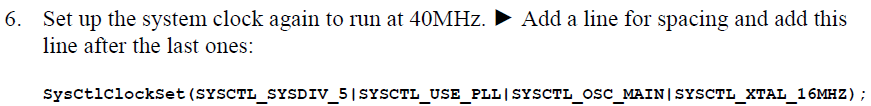
Plus I connected a single-turn potentiometer to PE3 and changed the clock setting to
SysCtlClockSet(SYSCTL_SYSDIV_5|SYSCTL_USE_PLL|SYSCTL_XTAL_16MHZ|SYSCTL_OSC_MAIN); .//40MHz
While sending data to UART, I recieved a error message from CCSv6.
CORTEX_M4_0: Error: Timed out while waiting for target powerup/polling a hardware resource.
What might be the problem?
Other forum(Stellaris forum) show similar problems like this. The suggested answer was
use SysCtlLDOSet(SYSCTL_LDO_2_75V); .
(Link : http://e2e.ti.com/support/microcontrollers/stellaris_arm/f/471/t/170954.aspx )
However, Tiva doesn't give API related to control LDO doesn't it?
What should I do..?
Regards, Min-Ku.