This thread has been locked.

If you have a related question, please click the "Ask a related question" button in the top right corner. The newly created question will be automatically linked to this question.

Interfacing SST25VF016B SPI with TM4C1230H6PM is not working

Other Parts Discussed in Thread: TM4C1230H6PM

Hi,

    I am interfacing SST25VF016B with Tiva Series TM4C1230H6PM. I am trying to read the JEDEC ID from serial flash SST25VF016B but i have received only 00 00 00. And i have noticed, the SO Pin is not sending out any data.
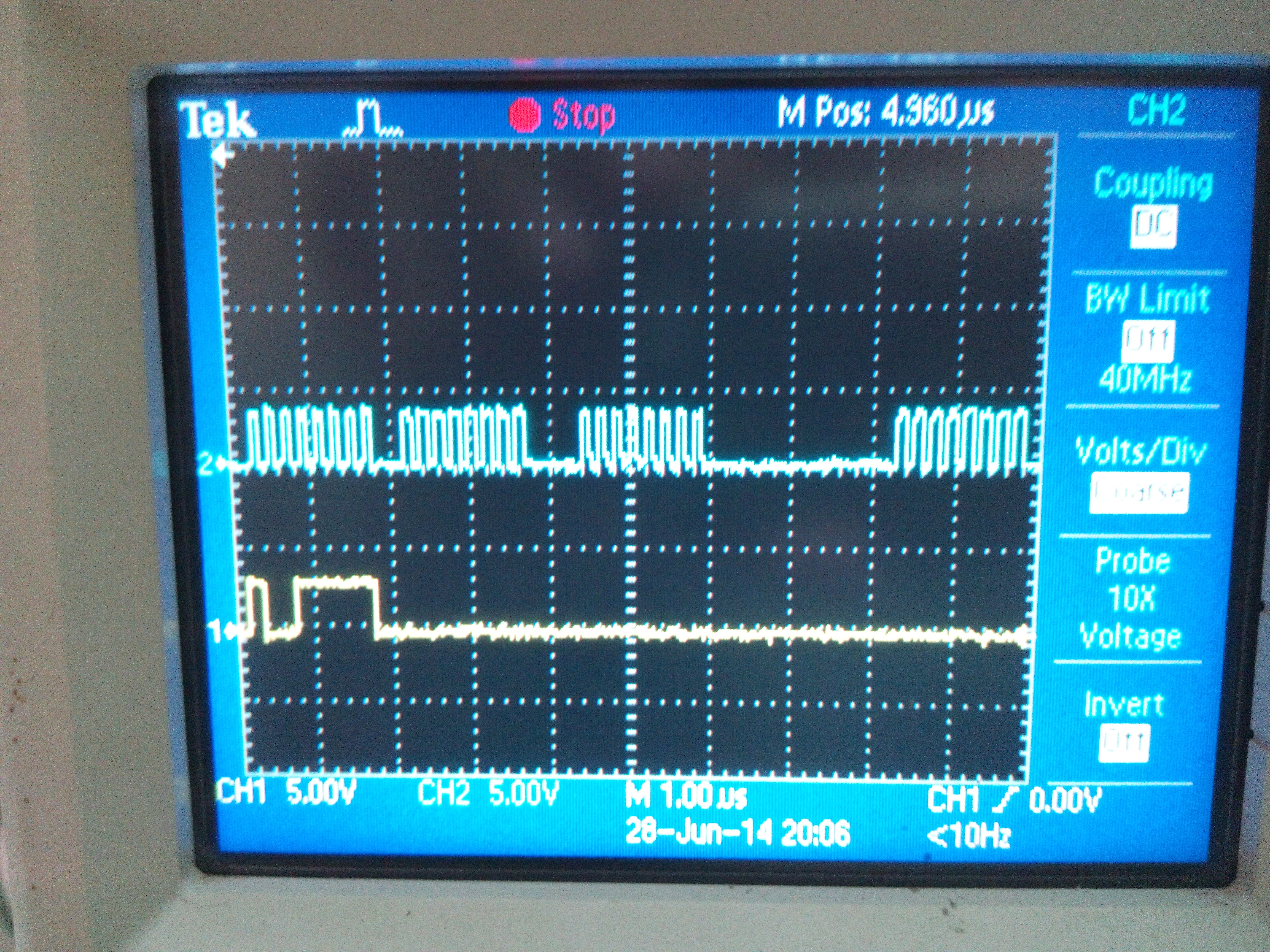
I am using 10 MHZ system clock. I can able to generate the clock.   I checked in CRO and the read instruction (0x9F) is going fine and i saw the clock also working fine. the problem here is serial is not sending any data on SO Pin. Please guide me. I have attached the snap shot of CRO signals.

 void Configure_SPI(void)
{
        uint32_t clk=0;
        char buf[10];
        //
    // The SSI1 peripheral must be enabled for use.
    //
    SysCtlPeripheralEnable(SYSCTL_PERIPH_SSI1);
        //SysCtlPeripheralEnable (SYSCTL_RCGC1_SSI1);


    //
    // For this example SSI1 is used with PortD[0:3].  The actual port and pins
    // used may be different on your part, consult the data sheet for more
    // information.  GPIO port D needs to be enabled so these pins can be used.
    // TODO: change this to whichever GPIO port you are using.
    //
    SysCtlPeripheralEnable(SYSCTL_PERIPH_GPIOD);
    
        GPIOPinTypeGPIOOutput(GPIO_PORTD_BASE, GPIO_PIN_1); //SSI1Fss
        GPIOPinWrite(GPIO_PORTD_BASE, GPIO_PIN_1, GPIO_PIN_1);
        //
    // Configure the pin muxing for SSI1 functions on port D3, D2, D1, and D0.
    // This step is not necessary if your part does not support pin muxing.
    // TODO: change this to select the port/pin you are using.
    //
    GPIOPinConfigure(GPIO_PD0_SSI1CLK);
    GPIOPinConfigure(GPIO_PD2_SSI1RX);
    GPIOPinConfigure(GPIO_PD3_SSI1TX);
        
        //
    // Configure and enable the SSI port for SPI master mode.  Use SSI1,
    // system clock supply, idle clock level low and active low clock in
    // freescale SPI mode, master mode, 1MHz SSI frequency, and 8-bit data.
    // For SPI mode, you can set the polarity of the SSI clock when the SSI
    // unit is idle.  You can also configure what clock edge you want to
    // capture data on.  Please reference the datasheet for more information on
    // the different SPI modes.
    //
        clk = SysCtlClockGet();
        sprintf (buf,"%d",clk);
        UartSend5(buf);
    ROM_SSIConfigSetExpClk(SSI1_BASE, SysCtlClockGet(), SSI_FRF_MOTO_MODE_0,
                                                      SSI_MODE_MASTER, 5000000, 8);
        

    //
    // Configure the GPIO settings for the SSI pins.  This function also gives
    // control of these pins to the SSI hardware.  Consult the data sheet to
    // see which functions are allocated per pin.
    // The pins are assigned as follows:
    //      PD3 - SSI1Tx
    //      PD2 - SSI1Rx
    //      PD1 - SSI1Fss
    //      PD0 - SSI1CLK
    // TODO: change this to select the port/pin you are using.
    //
        GPIOPinTypeSSI( GPIO_PORTD_BASE,GPIO_PIN_0| GPIO_PIN_3 | GPIO_PIN_2 );
        
    
        // HWREG (SSI1_BASE + SSI_O_CR1) |= SSI_CR1_LBM;
    //
    // Enable the SSI1 module.
    //
    SSIEnable(SSI1_BASE);
        
}

void EnableDevice()
{
    GPIOPinWrite(GPIO_PORTD_BASE, GPIO_PIN_1, GPIO_PIN_1);             /* enable device */
    delay_ms (100);
    GPIOPinWrite(GPIO_PORTD_BASE, GPIO_PIN_1, 0);             /* enable device */
    //delay_ms (100);
    //GPIOPinWrite(GPIO_PORTD_BASE, GPIO_PIN_1, GPIO_PIN_1);
    delay_ms (100);
}

unsigned long Jedec_ID_Read(void)
{
    uint32_t temp,temp1,temp2 ;
    char buf[10],b uf1[10],buf2[10],buf3[3];
    temp = 0;temp2=0;temp1=0;

    GPIOPinWrite(GPIO_PORTD_BASE, GPIO_PIN_1, 0);             /* enable device */
    delay_ms (100);

    SSIDataPut (SSI1_BASE,0x9F);         /* send JEDEC ID command (9Fh) */
    
    
    SSIDataPut(SSI1_BASE,0x00);
    SSIDataGet (SSI1_BASE, &temp2);
    sprintf (buf1,"%x",temp2);


    SSIDataPut(SSI1_BASE,0x00);
    SSIDataGet (SSI1_BASE, &temp2);
    sprintf (buf2,"%x",temp2);


    SSIDataPut(SSI1_BASE,0x00);
    SSIDataGet (SSI1_BASE, &temp2);
    sprintf (buf3,"%x",temp2);


    delay_ms (50);
    GPIOPinWrite(GPIO_PORTD_BASE, GPIO_PIN_1, GPIO_PIN_1);             /* disable device */
    delay_ms (100);

    sprintf (buf,"%x",temp2);
    return temp;
}

int main ()

{

             SysCtlClockSet(SYSCTL_SYSDIV_2_5    | SYSCTL_USE_PLL | SYSCTL_OSC_MAIN | SYSCTL_XTAL_10MHZ);
        FPUEnable();
        
        ROM_FPULazyStackingEnable();

        Configure_SPI(); 

         EnableDevice ();
         delay_ms (100);
             Jedec_ID_Read ();

          return 0;
}

Please help me to come out of this issue.

Thanks,

Shanmugam

  • Feel your pain - yet a key point is very poorly detailed - complicates life for those seeking to assist.

    "SSI_FRF_MOTO_MODE_0" reveals only under a "code search" - it is significant - is it not?  Your MCU has much more set-up flexibility than your SPI Slave.  And you must carefully "mate" your MCU's SPI mode to that "required" by your slave.  And - you're completely silent as to that.

    Our group always advocates for KISS.  SPI chip family you employ frequently torments new users - it is reasonably demanding.  Suggest that you build confidence via simpler, small capacity SPI eeprom.  (I bet you will learn/profit from that exercise) 

    While you're rightly focused upon your failed SPI transaction - do many/most of your other MCU peripherals behave to expectation?  (we're not told)  It assists greatly when such detail arrives initially, crisply, cleanly - saves wear/tear of interrogation, other guess-work...

  • Hi,

    Thanks for the reply.

    I am using Freescale SPI format, SPO = 0 and SPH = 0. i have tried Microwave format also but no luck.

    I have attached the registers values of SSI1 also. I think this will to understand much more in detail.

    Can you please point me which point you need in detail. I am ready to give you the answer.

    Thanks,

    Shanmugam

  • My sense is that you do not (yet) fully grasp the slave device's "favored" SPI format.  (this indicated by your having "tried" other formats)

    Might it be best to open the slave's signal timing chart - and compare it closely, carefully - against those available w/in your MCU?  Vital that the CS's (SSxFS) arrival/departure and (SSxClk) clock edges are in full agreement.  (i.e. to be clear - both the signal timing & signal edges "agree" between the slave's timing drawing and that of the "best match" w/in your MCU manual)

    Have you done that?  (there should be no guesswork) Often the CS/SSxFS timing cannot be matched - in this event you have to liberate that pin from SSI - switching it instead into push-pull GPIO Output mode - and then controlling it manually. (i.e. via gpio function calls)

    Requested - but not yet presented - is your comment upon the correctness of any/all other MCU peripheral behavior.  This aids as the general MCU operation must be established/verified - otherwise much time/effort falls into "bottomless pit."  (and - of course - it's hoped that your concern for your helpers drives you to prevent this...)

    No response to the suggestion of KISS - (your acquisition of far simpler, small SPI eeprom, to better build/ease your SPI understanding/mastery prior to your assault upon the (far more) complex SPI device...)

    And - along further KISS lines - your attempt to, "read the JEDEC ID" might require some, "special" handling.  (I've not read the SPI data (yet) prefer to await poster's basic compliance)  Most always it proves easier to "write" to the SPI Slave than to read from the device.  (and you may have chosen a more complex "read" w/out first having achieved the more basic...  although we're never told if you enjoyed any success beyond the failure to, "JEDEC ID" as (apparently) your first attempt!)  Very non-KISS!  (and - predictable results emerge...)