Other Parts Discussed in Thread: LMP90100
Hi TI,
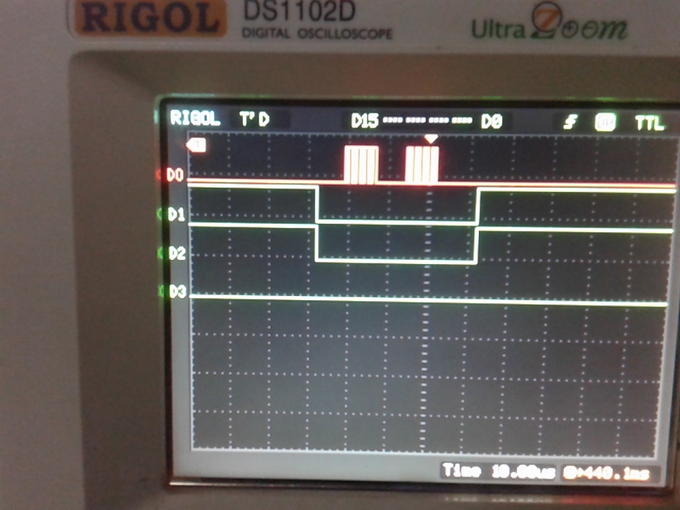
i AM using tm4c1230 series controller i want inter face with lmp90100 AFE ,ssi communication i configured but am not getting how to give ura address someone can help me
Other Parts Discussed in Thread: LMP90100
Hi TI,
i AM using tm4c1230 series controller i want inter face with lmp90100 AFE ,ssi communication i configured but am not getting how to give ura address someone can help me