This thread has been locked.

If you have a related question, please click the "Ask a related question" button in the top right corner. The newly created question will be automatically linked to this question.

Tiva DMA limitations?

Other Parts Discussed in Thread: TM4C1294NCPDT, TLC5940, ENERGIA, CC3200

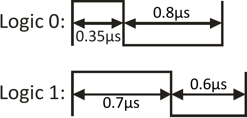
I'm trying to control a WS2812. For this i found that using DMA triggered by timers to control GPIO is the best way to go.

Since i never used DMA i need some info.

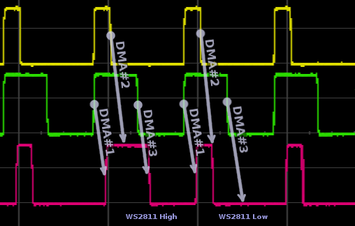
The idea is to use 3 timers. 1 triggers a 0xFF transfer, the 2nd triggers data(it varies) transfer, the 3rd triggers 0x00 transfer. This is all transfered to a GPIO wich controls all 8 ports. My question is, can't i have another DMA chanel do the same to another GPIO at the same time or realy quickly after the transfer to the 1st GPIO?

  • The idea is to do the signals above

    Ok so i think i got it

    I enable 3 DMA chanels.

    I enable 2 split pair timers in PWM pode with the right duty and with both edge interrupt for one that triggers #1 and #3 and falling for the one that loads DMA #2

    I can only trigger a specific chanel with each Timer right?  i have to respect the table on page 680 (tm4c1294ncpdt)

    I should be able to change the DMA chanel a timer trigers in the interrupt right?

    Ok, now the destination, can i chose any chanel to any peripheral destination?

  • Hello Luis,

    That is correct. The DMA channel is fixed for most modules, with only some modules having more than one mapping in the table. You can change the DMA Channel a timer triggers anywhere in the code as long as it has mapping to the timer trigger.

    For transferring of data DMA can send data to any other peripheral as long as the Peripheral is enabled and configured correctly.

    Regards

    Amit

  • Thanks! Amit to the rescue, as always. In 9.2.1 of the datasheet maybe it should be more clear by simply adding a word no?

    Each DMA channel has up to nine possible  trigger assignments

    So about the trigger.

    I can configure the DMA to burst mode, arbitration 1, with 8 bit transfers. Then trigger a 8bit transfer every rising edge of the split timer? 

    Also for the 3 transfers is need, can i use 3 memory transfer, with 3 channels, to the GPIO with both rising and falling edges of a timer, for transfer #1 and #3? or do i have to interrupt the timer to change the chanel source memory address it triggers for that?

    If i have a uint8_t values[20000]  does the DMA transfer each member of the array at the time (values[0], vallues[1],etc)? If i have a uint32_t values[1000] does it transfer values[0] first byte, then 2nd, 3rd and 4th, and only then goes to values[1]?

  • Hello Luis,

    The full statement from the TM4C129 data sheet is

    Each DMA channel has up to nine possible assignments which are selected using the DMA Channel
    Map Select n (DMACHMAPn) registers with 4-bit assignment fields for each μDMA channel

    For transferring the 3 data locations, you need to configure the single channel for the timer trigger to do 3 total transfers in arbitration of 1 unit. No need to change the channel.

    The uDMA will transfer in terms of number of Arbitration Size for every trigger. So it all depends on what the total size of transfer is and the Arbitration Size programmed. Only in Auto Mode will it transfer all the data in one shot. Do remember the maximum size for transfer by uDMA is 1024 locations.

    Regards

    Amit

  • Hi Amit

    I want to do 3 transfer cycles. This is to make the waveform i need with the GPIO, and i need to do this transfer multiple times. 1st is always 0xFF, 2nd varies, 3rd is always 0x00. So, to avoid using more ram, i wanted to the 1st and 3rd to always transfer the same memory location.

    Maybe this will explain better what i want to achieve

    the 1024 limits the number of 8bit transfers? Also one thing i still don't get, mainly because i don't know how ARM handles RAM access. If i have a uint32_t value[4]. Will the 8 bit transfer, with a arbitration of 4, tranfer the 32bits of value[0]? or transfer the first 8 bits of value[0] and then transfer the first 8 bits of value[1]?

    Also, wich event triggers the DMA with the timer? Rising or falling edge?

  • Ok so here is my idea.

     i use for example 1st timer rising edge to trigger DMA.

    2nd timer falling edge to trigger 2nd timer DMA

    use a GPIO input to trigger DMA on 1st timer falling edge.

    So for this too work i need to

    First find out wich edge triggers the DMA with the timer and if i can configure it.

    Second, find out if can with a DMA trigger always send the same memory address without processor intervention for 1st and 3rd DMA transfer.

    Third, find out how i need to organize data for the 2nd DMA transfer. 

  • Hello Luis,

    The timer does not have rising or falling edge. It has trigger based on timer timeout event or on timer match event.

    To read 1st and 3rd from the same location. you would need to do a Peripheral Scatter Gather (which is complicated to debug if uDMA is not configured correctly or the sequence of trigger is not correctly done)

    Regards

    Amit

  • From the datasheet it seems i could use the timer in PWM mode to trigger DMA. So can't i set it like a interrupt to see if it's a rising or falling edge?

    Hum, in PWM mode the match interrupt occurs when the PWM output changes from 1 to 0 right?

  • Hello Luis,

    Now that clarifies. And the solution you have would need a modification as follows

    Each of the sub timers have their own independent dma channel mapping

    Timer-A channel which is always on falling edge will perform only 1 transfer (Called Transfer #2) with ARB Size of 1 and Transfer Size of 1.

    Timer-B channel which is always on both edge will perform only 1 transfer (Called Transfer #1) on the first edge and only 1 transfer (Called Transfer #3) on the second edge. The ARBsize will be 1 and total transfer size will be 2,

    On DMA Done for each channel the source data will be re-initialized by the CPU. Of course both channels on DMA request will transfer from memory to GPIO.

    Amit

  • As always thank you very much for your help Amit.

    What you sugest setting the TimerA for falling edge only and TimerB for both edges.

    Considering i would be using basic mode, i would need a memory buffer for TimerA and other for TimerB. The buffer max size is 1024 transfers right? Problem is i would have a uint8_t buffer1[1024] full of the same value only, always 0xFF right?

    For buffer2 can i use a uint16_t and transfer 8bits at a time? like: 0x00XX being X the value i need to change with the CPU every cycle. 

    Now i'm just trying to save up RAM space, since i only need 8 variable bits per transfer. But i think this will do just fine, with 512 transfer per CPU initialization ( because of needing 2 transfer size for the TimerB)

  • Hello Luis,

    No. buffer1 can be declared as buffer1[1] with the value of 0xFF and then on completion the DMA channel enabled in the control word by writing the value of BASIC in Transfer Type

    Buffer2 can be declared as buffer2[2] with the [0] containing 0xXX and [1] containing 0x00. And on DMA Done the same operation as above done for Control word of the second channel.

    Regards

    Amit

  • i see. But won't this add alot of overhead, interrupting when DMA done and enabling it again? There seems to be a tradeoff overhead vs memory usage i need to make.

    Also, in buffer2, the 0xXX is a table of hundred of values of this type. For lower overhead it seems beter to use declare buffer2 with 1024 members for a efective use of 512 full data. 

    To make the methods your sugesting i need it to done with hardware, it seems possible with gather-scater, of course that seems much more complicated. By my math, i won't be short in RAM. 64 LEDs * 8 outputs * 24 bytes = 12288 Bytes, wich is fine. Even if i can make it 32 outputs it's less than 50Kb. If i have low ram then i will try scater-gather

    You have been most helpfull Amit as always. Great work you have been doing here in support forums.

  • In uDMAChannelControlSet i read this from the peripheral guide:

    "Choose the source address increment from one of UDMA_SRC_INC_8,
    UDMA_SRC_INC_16, UDMA_SRC_INC_32, or UDMA_SRC_INC_NONE to select an
    address increment of 8-bit bytes, 16-bit half-words, 32-bit words, or to select non-incrementing."


    This means if i chose a arbitration size of 1024 and set source address increment to UDMA_SRC_INC_NONE then i can use a variable uin32_t FirstValue = 0xFF.

  • I made a test code to control 1 ws2812 in wich i was had no sucess.

    Maybe i am undestanding sometigh rong abou the DMA.

    If you could help it would be much apreciated

    3324.teste_ws2812_DMA.rar

  • Hello Luis,

    Selecting Arb Size of 1024 with UDMA_SRC_INC_NONE is perfectly fine. However the meaning changes with the number of transfers. For any transfer size it since ARB > TRANSFER SIZE, all the data from the Source Buffer would be sent out on the trigger.

    I will have a look at the project you have done next week.

    Eventually the DMA will give a done signal, so the overhead v/s memory size is something that you have to look at. Having a larger memory size would mean that the time spent by the CPU to update a buffer and then enable the channel again would be slightly lesser. For a fixed buffer value like 0xFF, it would be significantly lesser. But for a changing buffer value the optimal size of the buffer is critical as the DMA triggers will be coming every N us and the CPU needs to re-write the buffer and enable the channel before that.

    Regards

    Amit

  • It seems i'm getting there. The code still doesn't work, i'm missing sometigh key about the DMA. That's always the problem with using new peripherals especialy such complex ones. But o well, it's comes with the vocation.

    Thanks. I really want to learn to use such a powerfull feature of ARM to utilize all the peripherals at maximum speed. Have a nice weekend

  • Hello Luis

    Appreciate the discussion we had and especially the effort you have put in to it.

    As I mentioned earlier, if I can make a project out of it to mimic what you are trying to do, I would surely post the code.

    Regards

    Amit

  • Just want to point out some info about performance math. This is important since i want to know if this is viable. If anyone see i have made  horrible mistake please say so (my grammar doesn't count)

    I found out the ARM that are used to control WS2812 this way have a DMA with a transfer counter up to 15bits thus using less of the CPU in big transfers.

    The TM4c1294 being a MCU with 256kB ram, at leas 4x greater than those MCUs, would beneficiate alot from a DMA with a bigger transfer counter, maybe sometigh to consider in a future design?

    Still, i'm using Tiva, due to it's speed. Interrupts have a minimum time of 180nS and in some test controling other driver (TLC5940), i had critical interrupts too and go them down to 400nS and never going over 1,5uS and that was with a pretty busy interrupt. So having a max of 512 wave outputs (due to the 0x00 transfer), i can control 21 LEDs in each DMA cycle. So 24bits per led, times 21 leds, time 1,25 wich is the time of 1 bit makes 640uS,  1,5uS/640uS= 0,3% processor ocupied. 

    Well dam, i got  0,3% of the processor ocupied each DMA cycle, seems i can't the new call of duty on my Tiva. Doesn't seem the smaller DMA 10bit transfer counter will cause problems.

  • Hello Luis,

    I am not sure I follow the equation. If the transfer has to be done multiple times over and over again, the CPU overhead of re-initializing the uDMA Channel Structure also needs to be accounted for in the equation?

    Regards

    Amit

  • Hi Amit, sometimes i am not clear with my thiking, everytigh i write seems to make sense even if detail lacks since well, it's in my head. Sorry about that

     imagen the need to control 84 ws2812. I need 4 DMA transfers due to the fact that each DMA burst can only send data for 21 of them.

    Well then i have a array ready with data for the 84 ws2812. I just need betwen DMA transfers to change the starting address of the source. At the end of the 4 DMA transfers, a full data transfer, i stop this cycle and the processor can load the data array with new values and set up the DMA again.

    As i said, while in doing a full data transfer, for all the ws2812, the cpu will be asked every 630-640uS to spend 1,5uS setting up the DMA for the next partial transfer, accounting from timing test done before, The 1,5uS time is just a estimate but i belive i won't take more than 3uS. Of course after a full transfer, to update the array to new values will take longer 

  • Hello Luis,

    I do understand the ~1.5us and the 24-bit pattern per LED. But how do you plan to control the 84 WS2812 with 8-pins. That is what not becoming clear.

    UPDATE START---

    The code file that you sent is not complete. I am not sure what the sequence of initialization have to be for it.

    UPDATE END---

    Regards

    Amit

  • Hi Amit thanks for keeping helping me

    Ok how about 8 pins control 84 leds: they don't, at least in the example i said. It's just 1 pin that control 84 leds. Since the DMA transfers 1 byte each time, it's changing the 8 pin data right? So if i make it possible to control 84 leds from 1 pin, then it would be possible to contrl 84*8 Ws2812 with the 8pins.The idea it's i have paralel control of varios Ws2812. Maybe i'm not clea about sometigh, i'm sorry about that, you know the TLC5940, you can cascade them in series? The ws2812 as a similar fuctionality. i'm sorry i didn't say that.

    Here is the datahseet http://www.adafruit.com/datasheets/WS2812.pdf

    Incomplete? i made it looking at the DMA example in tivaware folder. Hum gona thave to check it out. In that example i just try to send data to 1 ws2812 (times 8 since i'm controling 8 pins at the same time right?)  and then stop. 

  • Hello Luis,

    OK. Now I get it. 1.5us*24*21 (since you would be having 21 in cascade).

    Without a circuit diagram and the lack of a IDE project, that I could compile and run with the same settings you have it becomes difficult at time. So, I would but naturally ask questions.

    The rar file that was sent only had one file and not like a Project for the IDE you may be using with the startup.c, compilation swithces, etc. That is why I mentioned it to be incomplete.

    Regards

    Amit

  • Hi Amit, it's normal for you to ask questions especialy when i don't provide full information.

    The code is complete because i use Energia to avoid problems with startup files and includes. i'll download CCS and import it to CCS and post that file here, luckyli CCS now suports Energia projects

  • Hello Luis

    No problem. I have started working on a non-Energia based code in CCS, that you may use a reference

    Hope to get it done by next week.

    Regards

    Amit

  • Thanks alot Amit!

    With only PIC and Arduino users in my college it's hard to learn such complexe programing with Tiva. But with TI i always find great support to learn, much better than most. And i realy like cheap and powerfull ARM platforms like Tiva

    Of course i won't give up trying to get it working even before your example

  • By the way, is there a Tiva with bigger DMA transfer counter? I think i have a way to get arround that limitation if the DMA can transfer data to the transfer counter register but i would be nice to know

  • Hello Luis,

    I think using the PWM module would be a better solution that using timers. I will shortly let you know how after I am done with the code

    Regards

    Amit

  • The PWM module doesn't have a DMA chanel.  So i would have to conect a PWM to a GPIO and use it to trigger the DMA... problem is would need 2 GPIO module, or maybe use the 2 ADC module

  • Hello Luis,

    Here you go. The only thing you need to do on the board for TM4C129 is to connect the PF0 to PF1. You can view the output on PE pins.

    http://e2e.ti.com/cfs-file.ashx/__key/communityserver-discussions-components-files/908/6507.TM4C129_5F00_UDMA_5F00_WS2812.7z

    Regards

    Amit

  • Hi Amit,

    Well done. I've got this to work with some WS8211 (these have the same data frame as the WS8212 but are 12v). 

    I have a few questions, but first a few comments for those trying to get this to work.

    For the rand function to work add #include <stdlib.h>. Also there is no gap between the data being sent, so there is no reset being established with the LEDs, so I believe this means the chip will not use the data that has been sent. I just removed the ground for a second and put it back on, and this then changes the color of the lights.

    Questions:

    I could only get 6 LEDs/Chips to light up, and it made no difference what I set the #define WS2812_BUF_SIZE 128*3  to. Possibly this has to do with the space/reset no being present....not sure.

    I am not sure I understand the purpose of the ping pong? In my application I have a large array filled with my light data called lightData[1500]  (this is enough data for 500 LEDs/chips). There is a lot of work performed before creating the light data as there are algorithms creating different lighting effects. 

    Can I use the technique you have presented with my lightData array? 

    Glenn.

  • Hello Glenn,

    The rand function was meant only for my testing. In your case you would need to replace every N*3+1 element of the ping-pong buffers with the actual data.

    Since I do not have WS8212 I cannot readily test it but surely you can. Please do note that the DMA will not accept anything more than 1024 transfer size.

    Regards

    Amit

  • Hi Amit,

    Not sure I fully understand.

    Is it possible to get this to work with my data (lightData[1500] Array), which is larger than 1024? 

    Perhaps the question is, do I need to use DMA, or can I use my data that is stored in a statically declared global array that I refresh with data using a timer (TI-RTOS Clock)?

    Glenn.

  • Hello Glenn,

    If CPU is not going to done anything else but send the data, then a RTOS Clock or for that purpose timers are good enough.

    for using the uDMA, you can split the array into 2 parts. Ping doing 750 and Pong doing 750 entries of the array.

    Regards

    Amit

  • Hi Amit,

    I just use the RTOS Clock to trigger a completely new set of data, I am not using it for sending individual packets of data. I use the RTOS Clock to control the speed the light effect looks like (for example I can speed up or slow down a chase effect ).

    This is my currently process:-

    1. Clock Trigger (trigger the selected effect with selected parameters (colors, speed, brightness))
    2. Create New lightData[] 
    3. Create Manchester Encoded data from byte n
    4. Send word out SPI MOSI
    5. Return to step 3 until there is no more lightData to send

    ..................

    I have looked at your code and cannot work out how I can get the PWM to use my array data, and not uDMA.

    For example, I have the following array, which represents 3 separate lights/chips of Red, Green and Blue

    static uint8_t lightData[9] = { 0xFF, 0x00, 0x00, 0x00, 0xFF, 0x00, 0x00, 0x00, 0xFF};

    Where/How would I get the PWM in your code to use this array data instead of the uDMA data?

    Thanks again, I really appreciate you sharing your expertise in assisting me solve this problem!

    Glenn.

  • Hello Glenn,

    I thought about this approach as well, and it would be a complicated solution.

    Anyways in the original code I sent, the following is the place where rand has to be replaced by the value you have to send.

            if((ui32Index%3) == 1)
            {
                g_ui8TxBufA[ui32Index] = rand()%256;
                g_ui8TxBufB[ui32Index] = rand()%256;
            }

    Regards

    Amit

  • Hi Amit

    Realy nice code,  never thought of using other DMA modes.

    I think i'm starting to get what you did.

    You used the PWM module to generate in PF0 a PWM signal. This signal is always low and fires at 0,35us and 0,7uS, i also didn't know about this feature of the PWM module, everytigh i used before has always just 1 positive and 1 negative side per period. With that i can use a single GPIO to send eveytigh

    In this mode of course i have to use 3x more RAM for each bit, alas this is the hardest part to optimize, but i think i can work with it. Also here i have to update the buffer betwen PING and PONG, that will make some overhead surely.

    Again thank you very much. I think i can progress from here.

  • Hello everyone

    So i am probabl having a newbiew moment but, in the code provided i can't see in the main code the variable g_ui32TxBufACount changing. It's always 0 it seems.

    I'm using while(g_ui32TxBufACount < 4) to check. Just this bit isn't working for me yet. It's updating the values sucessefuly

    Edit:

    I have another code with some changes to better acomodate my needs, but your code helped so much. I still haven't decided wich method is better to run processing of other things in the background but i found sometigh interesting: 

    BASIC mode can be programmed to ignore when XFERSIZE reaches 0x000 and continue copying
    on request until the channel is stopped manually. If the NXTUSEBURST bit in the uDMA Channel
    Control Word (DMACHCTL) register is set while in BASIC mode and the XFERSIZE reaches 0x000
    and is not written back, transfers continue until the request is deasserted by the peripheral.

    Wich means i can have a timer counting the PWM signal and stop the DMA at a certain value, making the 1024 limit non existant.

  • Amit Ashara said:

    Anyways in the original code I sent, the following is the place where rand has to be replaced by the value you have to send.

            if((ui32Index%3) == 1)
            {
                g_ui8TxBufA[ui32Index] = rand()%256;
                g_ui8TxBufB[ui32Index] = rand()%256;
            }

    Thanks Amit, with your suggestions I am now able to use my lightData[] array to send data using this technique.

    However, it does require 1 byte stored in g_ui8TxBufA[] and g_ui8TxBufB[] for every bit of my lightData[], then you also have to store the additional bytes for %3=0 and %3=2. This effectively means I would need to use 184 (8*2*3) times the size of my lightData[] array, which means I would run out of memory very quickly on the TM4C123G.

    I will research this further and see if there is any way to optimize.

    Glenn.

  • Hello Glenn,

    I am not sure where the 8 and 2 comes from in the equation? Could you explain that?

    If I read the post correctly, then 3 is the number of bytes for 1 byte of data and 184 is the number of bits for the LED sequence?

    Regards

    Amit

  • Hi Amit,

    The 8 comes due to the situation that to get one PWM pulse of value 1, you need to set g_ui8TxBufA[ui32Index] to 0xFF.  The 2 comes due to the need to have 2 buffers g_ui8TxBufA[ui32Index]  and g_ui8TxBufB[ui32Index] 

    For example: 1 light requires 24 bits of data, so to set the LED to Red, you send FF0000. This then translates to 8 * 1bits (which is stored in g_ui8TxBufA as 8 * 0xFF) and 16 * 0bits (which is stored in g_ui8TxBufA as 16 * 0x00).

    This is what I needed to do to send the correct sequence of 1s and 0s.

    Glenn.

  • Hello Glenn,

    The minimum access size for uDMA is 8-bits. So for even one bit it needs to use a byte. Thus to send the 24-bits for one LED it would be 24*3 bytes. The 2 buffer size can be re-adjusted.so that each buffer sends one LED worth of data.

    Even with the equation you mentioned earlier it will translate to 8Kbytes which is something TM4C123 can accommodate in the SRAM.

    I would however let you make the decision based on the requirements you may be having...

    Regards

    Amit

  • Thanks Amit, 

    I appreciate all the expert assistance with this, your solution is very innovative and is likely to meet most peoples requirements, especially with the TM4C129 256kb RAM

    Unfortunately, the maximum number of lights that could be driven, due to the 32kb RAM on the TM4C123G would be about 400, due to other application memory requirements (most likely the number of lights would be a lot less, perhaps 200). The more lights the better, I am targeting 1000 or over if possible.

    Looks like I have 2 choices, either find an alternatively method that does not use uDMA or possibly migrate to the CC3200 which has 256kb of RAM, which makes things possible again....Then again the 1024 limit of uDMA makes things difficult.

    I think I need to revisit SPI and see if there is some combinations of speed and word size I can use to get things set up right. The advantage of SPI is that I can look at a bit in my lightData[] and then use a byte or even larger to represent it when sending it out, as this byte is only used during the sending of the SPI word, no need to build the entire buffer that has a byte per bit. The downsize to SPI is that it is difficult to recreate the required timing with the SPI speed setting and SPI word size (with for example 0b11100000 representing 1 and 0b11111100 representing 0)

    Glenn.

  • Hi Glen

    There's an option that uses less RAM but uses more peripherals. You could use 2 PWM signals. Conect 1 to 1 GPIO and other to 2 GPIO. The rising edge of the 2nd PWM would send a DMA request with a source address that doesn't increment, to send always 0xFF. The falling edge of the 1st PWM would send the data with Amit code, and the falling edge of the 2nd PWM would again send a fixed address with no increment to send always the value 0x00

    Edit:

    I do have a SPI code that controls the WS2812, but the DMA method seemed i could easily control more LEDs with less RAM. The problem with SPI is that you need 8bits of SPI data for every 1bit for the WS2812.

    I used a 6.4Mhz CLK for the SPI  and 8bit data packet.

  • i'm having a problem with the transfer counter.

    I've added this in the main code: 

      GPIOPinWrite(GPIO_PORTN_BASE, GPIO_PIN_0,GPIO_PIN_0);
      while(g_ui32TxBufACount < 1){
        GPIOPinWrite(GPIO_PORTN_BASE, GPIO_PIN_0,0); 
      }
      GPIOPinWrite(GPIO_PORTN_BASE, GPIO_PIN_0,GPIO_PIN_0);
    
      while(1);

    But it never leaves the while, no it's not in a infinite loop, it simply stops.it never leaves the while and only executes what's inside it 1-6 times.

    I've also added sometigh to make the transfer stop. "multiplica" is how many times i want the transfer to execute

          g_ui32TxBufACount++; //this alredy existed
    if( g_ui32TxBufACount>=multiplica){ GPIOIntDisable(GPIO_PORTF_BASE,GPIO_INT_DMA); PWMGenDisable(PWM0_BASE, PWM_GEN_0); return; }

  • Luis Afonso said:

    I do have a SPI code that controls the WS2812, but the DMA method seemed i could easily control more LEDs with less RAM. The problem with SPI is that you need 8bits of SPI data for every 1bit for the WS2812.

    I used a 6.4Mhz CLK for the SPI  and 8bit data packet.

    Ha! The reason I am looking into the PWM method is that I could not get a clock at 6.4Mhz on the TM4C123G, as it is 80Mhz, the divisions did not work....see the first line of my original post that brings me here - http://e2e.ti.com/support/microcontrollers/tiva_arm/f/908/t/358903.aspx

    I am imagining this is possible for the TM4C129? Or are you running approximately 6.4Mhz?

    It would be great to see how you have setup your timer and also how you represent 0 and 1 in binary and/or hex.

    -----------

    I may have a way around the 8bits of SPI data for every 1bit of WS2812. I am currently driving some 12bit chips that require Manchester Encoded data, and the method I am using will work for the 8bit WS2812 (Manchester Encoding is kinder, you only need to use 2 bits for every bit)

    Here is my code

    // Send the bits out using SPI
    	for (j = 0; j < 300; j++)
    	{
    		// Convert 8bit word into 16bit manchester encoded word
    		lightDataOutInt = me_encode_tab[lightData[j]];
    		SSIDataPut(SSI0_BASE, lightDataOutInt);
    	}

    /*
     * Copyright (c) 2005, Swedish Institute of Computer Science
     * All rights reserved.
     *
     * Redistribution and use in source and binary forms, with or without
     * modification, are permitted provided that the following conditions
     * are met:
     * 1. Redistributions of source code must retain the above copyright
     *    notice, this list of conditions and the following disclaimer.
     * 2. Redistributions in binary form must reproduce the above copyright
     *    notice, this list of conditions and the following disclaimer in the
     *    documentation and/or other materials provided with the distribution.
     * 3. Neither the name of the Institute nor the names of its contributors
     *    may be used to endorse or promote products derived from this software
     *    without specific prior written permission.
     *
     * THIS SOFTWARE IS PROVIDED BY THE INSTITUTE AND CONTRIBUTORS ``AS IS'' AND
     * ANY EXPRESS OR IMPLIED WARRANTIES, INCLUDING, BUT NOT LIMITED TO, THE
     * IMPLIED WARRANTIES OF MERCHANTABILITY AND FITNESS FOR A PARTICULAR PURPOSE
     * ARE DISCLAIMED.  IN NO EVENT SHALL THE INSTITUTE OR CONTRIBUTORS BE LIABLE
     * FOR ANY DIRECT, INDIRECT, INCIDENTAL, SPECIAL, EXEMPLARY, OR CONSEQUENTIAL
     * DAMAGES (INCLUDING, BUT NOT LIMITED TO, PROCUREMENT OF SUBSTITUTE GOODS
     * OR SERVICES; LOSS OF USE, DATA, OR PROFITS; OR BUSINESS INTERRUPTION)
     * HOWEVER CAUSED AND ON ANY THEORY OF LIABILITY, WHETHER IN CONTRACT, STRICT
     * LIABILITY, OR TORT (INCLUDING NEGLIGENCE OR OTHERWISE) ARISING IN ANY WAY
     * OUT OF THE USE OF THIS SOFTWARE, EVEN IF ADVISED OF THE POSSIBILITY OF
     * SUCH DAMAGE.
     *
     * This file is part of the Contiki operating system.
     *
     */
    
    #include "me_tabs.h"
    
    const unsigned short me_encode_tab[256] = {
    0x5555, 0x5556, 0x5559, 0x555a, 0x5565, 0x5566, 0x5569, 0x556a, 0x5595,
    0x5596, 0x5599, 0x559a, 0x55a5, 0x55a6, 0x55a9, 0x55aa, 0x5655, 0x5656,
    0x5659, 0x565a, 0x5665, 0x5666, 0x5669, 0x566a, 0x5695, 0x5696, 0x5699,
    0x569a, 0x56a5, 0x56a6, 0x56a9, 0x56aa, 0x5955, 0x5956, 0x5959, 0x595a,
    0x5965, 0x5966, 0x5969, 0x596a, 0x5995, 0x5996, 0x5999, 0x599a, 0x59a5,
    0x59a6, 0x59a9, 0x59aa, 0x5a55, 0x5a56, 0x5a59, 0x5a5a, 0x5a65, 0x5a66,
    0x5a69, 0x5a6a, 0x5a95, 0x5a96, 0x5a99, 0x5a9a, 0x5aa5, 0x5aa6, 0x5aa9,
    0x5aaa, 0x6555, 0x6556, 0x6559, 0x655a, 0x6565, 0x6566, 0x6569, 0x656a,
    0x6595, 0x6596, 0x6599, 0x659a, 0x65a5, 0x65a6, 0x65a9, 0x65aa, 0x6655,
    0x6656, 0x6659, 0x665a, 0x6665, 0x6666, 0x6669, 0x666a, 0x6695, 0x6696,
    0x6699, 0x669a, 0x66a5, 0x66a6, 0x66a9, 0x66aa, 0x6955, 0x6956, 0x6959,
    0x695a, 0x6965, 0x6966, 0x6969, 0x696a, 0x6995, 0x6996, 0x6999, 0x699a,
    0x69a5, 0x69a6, 0x69a9, 0x69aa, 0x6a55, 0x6a56, 0x6a59, 0x6a5a, 0x6a65,
    0x6a66, 0x6a69, 0x6a6a, 0x6a95, 0x6a96, 0x6a99, 0x6a9a, 0x6aa5, 0x6aa6,
    0x6aa9, 0x6aaa, 0x9555, 0x9556, 0x9559, 0x955a, 0x9565, 0x9566, 0x9569,
    0x956a, 0x9595, 0x9596, 0x9599, 0x959a, 0x95a5, 0x95a6, 0x95a9, 0x95aa,
    0x9655, 0x9656, 0x9659, 0x965a, 0x9665, 0x9666, 0x9669, 0x966a, 0x9695,
    0x9696, 0x9699, 0x969a, 0x96a5, 0x96a6, 0x96a9, 0x96aa, 0x9955, 0x9956,
    0x9959, 0x995a, 0x9965, 0x9966, 0x9969, 0x996a, 0x9995, 0x9996, 0x9999,
    0x999a, 0x99a5, 0x99a6, 0x99a9, 0x99aa, 0x9a55, 0x9a56, 0x9a59, 0x9a5a,
    0x9a65, 0x9a66, 0x9a69, 0x9a6a, 0x9a95, 0x9a96, 0x9a99, 0x9a9a, 0x9aa5,
    0x9aa6, 0x9aa9, 0x9aaa, 0xa555, 0xa556, 0xa559, 0xa55a, 0xa565, 0xa566,
    0xa569, 0xa56a, 0xa595, 0xa596, 0xa599, 0xa59a, 0xa5a5, 0xa5a6, 0xa5a9,
    0xa5aa, 0xa655, 0xa656, 0xa659, 0xa65a, 0xa665, 0xa666, 0xa669, 0xa66a,
    0xa695, 0xa696, 0xa699, 0xa69a, 0xa6a5, 0xa6a6, 0xa6a9, 0xa6aa, 0xa955,
    0xa956, 0xa959, 0xa95a, 0xa965, 0xa966, 0xa969, 0xa96a, 0xa995, 0xa996,
    0xa999, 0xa99a, 0xa9a5, 0xa9a6, 0xa9a9, 0xa9aa, 0xaa55, 0xaa56, 0xaa59,
    0xaa5a, 0xaa65, 0xaa66, 0xaa69, 0xaa6a, 0xaa95, 0xaa96, 0xaa99, 0xaa9a,
    0xaaa5, 0xaaa6, 0xaaa9, 0xaaaa, };
    const unsigned char me_decode_tab[256] = {
    0x0, 0x0, 0x1, 0x1, 0x0, 0x0, 0x1, 0x1, 0x2,
    0x2, 0x3, 0x3, 0x2, 0x2, 0x3, 0x3, 0x0, 0x0,
    0x1, 0x1, 0x0, 0x0, 0x1, 0x1, 0x2, 0x2, 0x3,
    0x3, 0x2, 0x2, 0x3, 0x3, 0x4, 0x4, 0x5, 0x5,
    0x4, 0x4, 0x5, 0x5, 0x6, 0x6, 0x7, 0x7, 0x6,
    0x6, 0x7, 0x7, 0x4, 0x4, 0x5, 0x5, 0x4, 0x4,
    0x5, 0x5, 0x6, 0x6, 0x7, 0x7, 0x6, 0x6, 0x7,
    0x7, 0x0, 0x0, 0x1, 0x1, 0x0, 0x0, 0x1, 0x1,
    0x2, 0x2, 0x3, 0x3, 0x2, 0x2, 0x3, 0x3, 0x0,
    0x0, 0x1, 0x1, 0x0, 0x0, 0x1, 0x1, 0x2, 0x2,
    0x3, 0x3, 0x2, 0x2, 0x3, 0x3, 0x4, 0x4, 0x5,
    0x5, 0x4, 0x4, 0x5, 0x5, 0x6, 0x6, 0x7, 0x7,
    0x6, 0x6, 0x7, 0x7, 0x4, 0x4, 0x5, 0x5, 0x4,
    0x4, 0x5, 0x5, 0x6, 0x6, 0x7, 0x7, 0x6, 0x6,
    0x7, 0x7, 0x8, 0x8, 0x9, 0x9, 0x8, 0x8, 0x9,
    0x9, 0xa, 0xa, 0xb, 0xb, 0xa, 0xa, 0xb, 0xb,
    0x8, 0x8, 0x9, 0x9, 0x8, 0x8, 0x9, 0x9, 0xa,
    0xa, 0xb, 0xb, 0xa, 0xa, 0xb, 0xb, 0xc, 0xc,
    0xd, 0xd, 0xc, 0xc, 0xd, 0xd, 0xe, 0xe, 0xf,
    0xf, 0xe, 0xe, 0xf, 0xf, 0xc, 0xc, 0xd, 0xd,
    0xc, 0xc, 0xd, 0xd, 0xe, 0xe, 0xf, 0xf, 0xe,
    0xe, 0xf, 0xf, 0x8, 0x8, 0x9, 0x9, 0x8, 0x8,
    0x9, 0x9, 0xa, 0xa, 0xb, 0xb, 0xa, 0xa, 0xb,
    0xb, 0x8, 0x8, 0x9, 0x9, 0x8, 0x8, 0x9, 0x9,
    0xa, 0xa, 0xb, 0xb, 0xa, 0xa, 0xb, 0xb, 0xc,
    0xc, 0xd, 0xd, 0xc, 0xc, 0xd, 0xd, 0xe, 0xe,
    0xf, 0xf, 0xe, 0xe, 0xf, 0xf, 0xc, 0xc, 0xd,
    0xd, 0xc, 0xc, 0xd, 0xd, 0xe, 0xe, 0xf, 0xf,
    0xe, 0xe, 0xf, 0xf, };
    const unsigned char me_valid_tab[256] = {
    0x0, 0x0, 0x0, 0x0, 0x0, 0x0, 0x0, 0x0, 0x0,
    0x0, 0x0, 0x0, 0x0, 0x0, 0x0, 0x0, 0x0, 0x0,
    0x0, 0x0, 0x0, 0x0, 0x0, 0x0, 0x0, 0x0, 0x0,
    0x0, 0x0, 0x0, 0x0, 0x0, 0x0, 0x0, 0x0, 0x0,
    0x0, 0x0, 0x0, 0x0, 0x0, 0x0, 0x0, 0x0, 0x0,
    0x0, 0x0, 0x0, 0x0, 0x0, 0x0, 0x0, 0x0, 0x0,
    0x0, 0x0, 0x0, 0x0, 0x0, 0x0, 0x0, 0x0, 0x0,
    0x0, 0x0, 0x0, 0x0, 0x0, 0x0, 0x0, 0x0, 0x0,
    0x0, 0x0, 0x0, 0x0, 0x0, 0x0, 0x0, 0x0, 0x0,
    0x0, 0x0, 0x0, 0x0, 0x1, 0x1, 0x0, 0x0, 0x1,
    0x1, 0x0, 0x0, 0x0, 0x0, 0x0, 0x0, 0x0, 0x0,
    0x0, 0x0, 0x1, 0x1, 0x0, 0x0, 0x1, 0x1, 0x0,
    0x0, 0x0, 0x0, 0x0, 0x0, 0x0, 0x0, 0x0, 0x0,
    0x0, 0x0, 0x0, 0x0, 0x0, 0x0, 0x0, 0x0, 0x0,
    0x0, 0x0, 0x0, 0x0, 0x0, 0x0, 0x0, 0x0, 0x0,
    0x0, 0x0, 0x0, 0x0, 0x0, 0x0, 0x0, 0x0, 0x0,
    0x0, 0x0, 0x0, 0x0, 0x0, 0x1, 0x1, 0x0, 0x0,
    0x1, 0x1, 0x0, 0x0, 0x0, 0x0, 0x0, 0x0, 0x0,
    0x0, 0x0, 0x0, 0x1, 0x1, 0x0, 0x0, 0x1, 0x1,
    0x0, 0x0, 0x0, 0x0, 0x0, 0x0, 0x0, 0x0, 0x0,
    0x0, 0x0, 0x0, 0x0, 0x0, 0x0, 0x0, 0x0, 0x0,
    0x0, 0x0, 0x0, 0x0, 0x0, 0x0, 0x0, 0x0, 0x0,
    0x0, 0x0, 0x0, 0x0, 0x0, 0x0, 0x0, 0x0, 0x0,
    0x0, 0x0, 0x0, 0x0, 0x0, 0x0, 0x0, 0x0, 0x0,
    0x0, 0x0, 0x0, 0x0, 0x0, 0x0, 0x0, 0x0, 0x0,
    0x0, 0x0, 0x0, 0x0, 0x0, 0x0, 0x0, 0x0, 0x0,
    0x0, 0x0, 0x0, 0x0, 0x0, 0x0, 0x0, 0x0, 0x0,
    0x0, 0x0, 0x0, 0x0, 0x0, 0x0, 0x0, 0x0, 0x0,
    0x0, 0x0, 0x0, 0x0, };
    

    6036.me_tabs.h

    I have attached the library, which does the translation. To make it work we would need to create a similar table for each possible 256 combinations of 1s and 0s in an 8 bit word. The part I still need to work out, would be that a 8bit value would create a 64bit word, and SPI only supports 32bit Words. 

    One way around this, and perhaps a much easier way is to use bitshifting, so you just send a bit at a time (read bit, select 8 bit representation of 0 or 1, send this as a 8bit SPI word),

    This method would also mean you would not need to create a large 256 translation table. As you just need to select between 2 different options (the 8 bit representation of 1 or 0). The only question is whether things would run quick enough...I am thinking it should.

    Glenn.

  • I actualy didn't check if it was 6.4Mhz, and yes i am using the tm4c1294xl launchpad

    I think i saw a PWM method before. After the falling edge, the DMA would load the next timer match value to change the period to match the data. I think the value for 800Khz is 150, at 120Mhz clock, so you would need a memory byte per each ws2812 bit.