This thread has been locked.

If you have a related question, please click the "Ask a related question" button in the top right corner. The newly created question will be automatically linked to this question.

Pin Usage from the Fuel Tank Booster Pack on Tiva Launchpad (EK-TM4C123GXL)

Other Parts Discussed in Thread: BQ24210, EK-TM4C123GXL

Which pin's are actually necessary for the Fuel Tank Booster Pack?

The example(examples/boards/ek-tm4c123gxl-boostxl-battpack) configures PD0 and PD1 as SCL and SDA pins for the fuel gauge IC.

    //
    // The I2C3 peripheral must be enabled before use.
    //
    ROM_SysCtlPeripheralEnable(SYSCTL_PERIPH_I2C3);
    ROM_SysCtlPeripheralEnable(SYSCTL_PERIPH_GPIOD);

    //
    // Configure the pin muxing for I2C3 functions on port D0 and D1.
    // This step is not necessary if your part does not support pin muxing.
    //
    ROM_GPIOPinConfigure(GPIO_PD0_I2C3SCL);
    ROM_GPIOPinConfigure(GPIO_PD1_I2C3SDA);

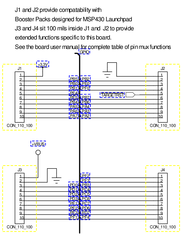
But when I overlap the header diagrams, SCL and SDA will actually connect to  PB6 and PB7. Am I missing something? See pins (12, 14) 

[Booster Pack Header Diagram] 

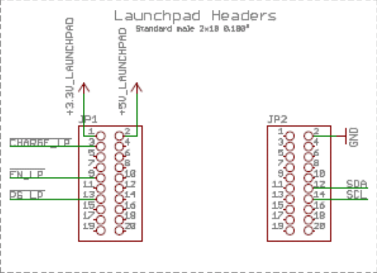
[Launchpad Header Diagram]

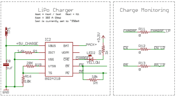
Additionally, it seems like resistors (0-ohms) R11, R12 and R13 are populated to enable 'charge monitoring', can I remove these to avoid conflicts if I decide to use the pins in their respective positions on the Launchpad? It seems like only R12 is a concern since it is tied to !EN pin. But I do not see any pins configured to control this pin in the example.  

Thanks,
Krithik

  • Hello Krithik

    In the schematic for EK-TM4C123 there are resistors R9 and R10 which connect PD0 to PB6 and PD1 to PD7 thus allowing PD0 and PD1 to work as I2C Lines.

    As for the other pins you mentioned how are they connected to the R11, R12 and R13? The corresponding pins from the booster pack will come to J1 of EK-TM4C123

    Regads

    Amit

  • Hello Amit, 

    Thanks for the reply. A complete oversight from my side, I was only looking at the schematic of the Booster Pack more closely. 

    I mean the R11, R12 and R13 resistors on the boosterpack. Sorry if there was any confusion. 

     I

    I see that they are connected to J1, but my concern is if there is any issue with leaving them floating after I remove those resistors. 

    !CHARGE_LP (R11) and !PG_LP (R13) are active low outputs that are simply there to monitor the status of the charging and power status. So I'm assuming there shouldn't be an issue, do let me know if there would be one. 

    But !EN_LP is an input tied to the host at PE4. Upon reading the datasheet for bq24210, the enable pin is connected to the host if it needs to enter suspend mode where it is neither charging or reverse conduction. The example doesn't seem to use this capability, hence the question. Should I simply tie the pad to ground? 

    Thanks,
    Krithik 

  • Hello Krithik,

    Not configuring the GPIO pins on the TM4C would also leave them in the same state. Otherwise the EK-TM4C123GXL or any interfacing document/code would have mentioned it.

    Regards

    Amit