This thread has been locked.

If you have a related question, please click the "Ask a related question" button in the top right corner. The newly created question will be automatically linked to this question.

LM4F120 unable to sync different timers

Hello everyone.

I know there are already some threads about timer sync, but I´ve tried all the suggested steps mentioned and i´m still not able to sync the timers i´m using.

I´m quite a noob on these matters, so please bear it with me.

A CCD project i´m working on requires quite some timers to obtain an image.

What i´m trying to do is to run, for now, 3 different timers.

My original configuration was:

Timer0 -> split pair, TimerA-pwm, with an interrupt

Timer1 -> split pair, TimerA-pwm, TimerB-oneShot with prescaler and an interrupt

Timer2->split pair, TimerA-pwm

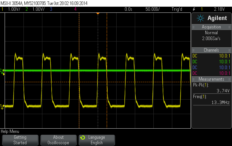
I had no sucess trying to sync Timer2_A with Timer1_A which is my final goal.

Later I learned that Timer0 must be used to sync other timers so i´ve changed the configuration so that Timer0 was there only to sync.

I´ve been changing the configuration of all the timers and trying different combinations but with no sucess.

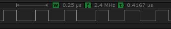
Now all I want is to sync Timer1 and Timer2, both running simple PWM in their A half with output in the respective pins and both with the same frequency and dutyCycle.

By sync i mean that their waveform should start at the same time so that later on i can change the dutyCycle in order to create a shift on the wave.

Here is an piece of my code for the timers:

        //act timers Peripherals
	SysCtlPeripheralEnable(SYSCTL_PERIPH_TIMER0);
	SysCtlPeripheralEnable(SYSCTL_PERIPH_TIMER1);
	SysCtlPeripheralEnable(SYSCTL_PERIPH_TIMER2);
	//
	TimerSynchronize(TIMER0_BASE, TIMER_1A_SYNC | TIMER_2A_SYNC );
	TimerSynchronize(TIMER0_BASE,0);

	//********************
	//act timers outputs
	GPIOPinConfigure(GPIO_PB4_T1CCP0);
	GPIOPinTypeTimer(GPIO_PORTB_BASE, GPIO_PIN_4);//timer1

	GPIOPinConfigure(GPIO_PB0_T2CCP0);
	GPIOPinTypeTimer(GPIO_PORTB_BASE, GPIO_PIN_0);//timer2

	//********************
	//type of timers config
	TimerConfigure(TIMER1_BASE, TIMER_CFG_SPLIT_PAIR| TIMER_CFG_A_PWM);
	TimerConfigure(TIMER2_BASE, TIMER_CFG_SPLIT_PAIR|TIMER_CFG_A_PWM);

	//********************
	//Timers_time config	
	TimerLoadSet(TIMER1_BASE, TIMER_A, 100 -1);
	TimerMatchSet(TIMER1_BASE, TIMER_A, 50 );

	TimerLoadSet(TIMER2_BASE, TIMER_A, 100 -1);
	TimerMatchSet(TIMER2_BASE, TIMER_A, 50);

	//********************
	//********************
	//act timers
	TimerEnable(TIMER1_BASE, TIMER_A);
	TimerEnable(TIMER2_BASE, TIMER_A);

Can anyone explain me what am i doing wrong?

Any suggestion are appreciated.

Thanks for your time. (pun intended)

  • Hello Andy,

    The Timer Synchronization must be done after the other timers have been enabled.

    Regards

    Amit

  • Hello Guru Amit :)

    Thanks for your answer.

    I could swear i tried declaring the sync after enabling the timers, but i´ve done so many changes that i can´t remember.

    It´s working now.

    Unfortunately I realize now that the shift in the wave i need to do requires the synced PWM to be inverted.

    I´ve checked the example invert.c included in the stellarisWare but i think the API commands there do not apply to the microcontroller i´m using (LX4F120H on a EK-LM4F120XL board).

    Could you explain me how to invert the output of the synced PWM or if that is even possible?

    I´m trying to check information about comparators and the up/down counting, as i seen in some posts on the forum.

    But, as usual, the configuration is going to be tricky.

  • Hello Andy

    The invert.c as far as I know is a PWM code and not a timer code. So pardon me, as I am now confused that you want to sync PWM or sync-timers?

    Regards

    Amit

  • Hello Guru Amit.

    You are right. I´m sorry for my inadequate use of terms.

    I did what i wanted, which is to sync 2 timers.

    But what those timers are doing is generating pwm signals on their pins. I thought that was the way to generate PWM on this microcontroller.Is it not?

    These images may illustrate what i´m trying to do;

    -----------------------------------These are the clocks i synced.

    -----------------------------------This is how i need the bottom clock to be.

    They both end at the same time.

    By explaining this i noticed that inverting wont solve my problem either because both clocks may end at the same time but opposite to each other.

    Can you give me any suggestion about how to accomplish what i want?

    I´ve seen some threads about dead band or comparators but i´m unsure about how to use that approach.

    Best regards.

    Andy

  • Hello Andy,

    I think the solution using the Timer for PWM would be to invert both the signals after setting the time base identical and the match value as per the low time of the PWM signals.

    I wish I had a scope to confirm my above statement.

    P.S: Stop adding "Guru"... Just Amit would suffice.

    Regards

    Amit

  • Oh, ok, no more Guru :)

    But, Amit, I still don´t know how to invert the output of a timer that is generating a PWM signal.

    If you could enlighten me, it would be great. Sorry for  being such a nag!

    And what do you mean you "wish you had a scope"? :P

    Best regards,

    Andy

  • Hello Andy

    You would need to set the register-bit GPTMCTL.TxPWML to invert the PWM output.

    What I meant was if I had a scope, I could have checked the function as per your requirement to ensure that it does work.

    Regards

    Amit

  • Thanks so much for you answer, Amit! I´ll start working on it right away.

    Yes :P I know the scope was meant to check if your solution worked, but i thought you were at TI, and so you should have a ton of instruments to work with...at least that was my idea...

    I´ve started coding the entire sequence of the timers, and unfortunately i´ve been running on some strange behavior from the one shotTimer (timer_B) which is mean to count the pulses of timer_A.

    This is still going to be a lot of work, so your help is very much appreciated.

    Best regards,

    Andy

  • Hello Andy,

    So is there a new code you are doing?

    Regards

    Amit

  • Hello, Amit!

    Not a new code, exactly, but a "construction" based on all the code i´ve been experimenting.

    Like i said before, to obtain an image from a CCD, a lot of clocks are needed. Some for the horizontal line pixels and others for vertical line pixels. You probably know that a lot better then I.

    I´ve taken all the experiments i´ve been doing with the timers (which are generating PWM clocks), including timer sync, and i´m now trying to reach the final code for the complete sequence of vertical and horizontal clocks which will enable the charge transfer from the CCD to an ADC.

    The ADC part i´ve haven´t thought of yet. But i know it will involve SPI communication. I´m hoping it will be easier then the clocks part.

    I´ve been testing code for the past hours and the strangest thing has happened (strange for me because i´m still learning).

    Allow me to post a piece of the code, but first i will describe how it works.

    I´ve been trying to write directly to the Timer Invertion register (GPTMCTL TnPWML )experimenting on syntax, because I don´t know how exactly do it nor where to perform such action (before or after the timers are enabled).

    I´ve tried things like the ones below and others that I eventually erased, but non of them worked.

    After working some more on the code I realize that Timer1 and 2 where being synced but did not start at the same point. Actually they start with the same offset every time.

    I don´t know why is that.
    But it allows me to change the the duty cycle of Timer2 making it exactly like i need it to be.

    Maybe you can find some way to describe that behavior with the code I´v posted.

    Basically what it does is to run pulses while it´s idle (Timer3 handler) and when i give the order it starts the sequence between horizontal and vertical clocks (PhotoPulses rotine)

    It does that 10 times and it generates groups of pulses according to Timer1_B OneShot count.

    Here is a screenshot of the last ms of the operation;

      (attempts to write to the inversion register)

    //HWREG(TIMER1_BASE + TIMER_CTL_TAPWML) = (1 << 14);//invert output pwm
    //HWREG(TIMER1_BASE + TIMER_CTL_TAPWML) = 0x01;
     //HWREG(TIMER1_BASE + (TIMER_CTL_TAPWML << 14)) = 1;//invert output pwm //HWREG(TIMER1_BASE + TIMER_CTL_TAPWML + (1 << 14)) = 1;

    void PhotoPulses()
    {
    
    	if (horizontalPulseRun < 10)
    	{
    		{
    			horizontalPulseRun++;
    			//SysCtlDelay(SysCtlClockGet()/1000/10);
    
    			GPIOPinWrite(GPIO_PORTE_BASE, XV1|XV2|XV3|XV4 , 16);
    			GPIOPinWrite(GPIO_PORTE_BASE, XV1|XV2|XV3|XV4 , 18);
    			GPIOPinWrite(GPIO_PORTE_BASE, XV1|XV2|XV3|XV4 , 2);
    			GPIOPinWrite(GPIO_PORTE_BASE, XV1|XV2|XV3|XV4 , 6);
    			GPIOPinWrite(GPIO_PORTE_BASE, XV1|XV2|XV3|XV4 , 4);
    			GPIOPinWrite(GPIO_PORTE_BASE, XV1|XV2|XV3|XV4 , 12);
    			GPIOPinWrite(GPIO_PORTE_BASE, XV1|XV2|XV3|XV4 , 8);
    			GPIOPinWrite(GPIO_PORTE_BASE, XV1|XV2|XV3|XV4 , 24);
    			GPIOPinWrite(GPIO_PORTE_BASE, XV1|XV2|XV3|XV4 , 24);
    
    			TimerEnable(TIMER1_BASE, TIMER_BOTH);
    			TimerEnable(TIMER2_BASE, TIMER_A);
    
    		}
    	}
    }
    
    void Timer1IntHandler(void)
    {
    	TimerIntClear(TIMER1_BASE, TIMER_TIMB_TIMEOUT);//reset interrupt
    
    	TimerDisable(TIMER1_BASE, TIMER_BOTH);//
    	TimerDisable(TIMER2_BASE, TIMER_A);
    
    	SysCtlDelay(SysCtlClockGet()/1000/20); //
    
    
    	//Timer1();
    	TimerLoadSet(TIMER1_BASE, TIMER_A, 100 -1);//
    	TimerMatchSet(TIMER1_BASE, TIMER_A, 50 );//
    	TimerLoadSet(TIMER1_BASE, TIMER_B, 17400/13);//
    	//Timer2();
    	TimerLoadSet(TIMER2_BASE, TIMER_A, 100 -1);//freq do timer
    	TimerMatchSet(TIMER2_BASE, TIMER_A, 50);//dutycycle
    
    	TimerSync();
    	PhotoPulses();
    }
    
    void Timer2IntHandler(void)
    {
    	TimerIntClear(TIMER2_BASE, TIMER_TIMA_TIMEOUT);
    }
    
    void Timer3IntHandler(void)//
    {
    	TimerIntClear(TIMER3_BASE, TIMER_TIMA_TIMEOUT);
    
    
    	if(pulse == 0)
    	{
    		GPIOPinWrite(GPIO_PORTB_BASE, GPIO_PIN_4 , 16);
    		GPIOPinWrite(GPIO_PORTB_BASE, GPIO_PIN_4 , 0);
    
    		GPIOPinWrite(GPIO_PORTE_BASE, XV1|XV2|XV3|XV4|XSHT , 48);
    		GPIOPinWrite(GPIO_PORTE_BASE, XV1|XV2|XV3|XV4|XSHT , 50);
    		GPIOPinWrite(GPIO_PORTE_BASE, XV1|XV2|XV3|XV4|XSHT , 34);
    		GPIOPinWrite(GPIO_PORTE_BASE, XV1|XV2|XV3|XV4|XSHT , 38);
    		GPIOPinWrite(GPIO_PORTE_BASE, XV1|XV2|XV3|XV4|XSHT , 36);
    		GPIOPinWrite(GPIO_PORTE_BASE, XV1|XV2|XV3|XV4|XSHT , 12);
    		GPIOPinWrite(GPIO_PORTE_BASE, XV1|XV2|XV3|XV4|XSHT , 8);
    		GPIOPinWrite(GPIO_PORTE_BASE, XV1|XV2|XV3|XV4|XSHT , 24);
    		GPIOPinWrite(GPIO_PORTE_BASE, XV1|XV2|XV3|XV4|XSHT , 56);
    	}
    	else
    	{//
    			GPIOPinWrite(GPIO_PORTE_BASE, XV1|XV2|XV3|XV4 , 16);
    			GPIOPinWrite(GPIO_PORTE_BASE, XV1|XV2|XV3|XV4 , 18);
    			GPIOPinWrite(GPIO_PORTE_BASE, XV1|XV2|XV3|XV4 , 2);
    			GPIOPinWrite(GPIO_PORTE_BASE, XV1|XV2|XV3|XV4 , 6);
    			GPIOPinWrite(GPIO_PORTE_BASE, XV1|XV2|XV3|XV4 , 4);
    			GPIOPinWrite(GPIO_PORTE_BASE, XV1|XV2|XV3|XV4 , 12);
    			GPIOPinWrite(GPIO_PORTE_BASE, XV1|XV2|XV3|XV4 , 8);
    			GPIOPinWrite(GPIO_PORTE_BASE, XV1|XV2|XV3|XV4 , 24);
    			GPIOPinWrite(GPIO_PORTE_BASE, XV1|XV2|XV3|XV4 , 24);
    
    			if(pulse == 1)
    			{
    				timer3Tick++;
    				if(timer3Tick > 50000)
    				{
    
    					timer3Tick = 0;
    					pulse = 0;
    					TimerDisable(TIMER3_BASE, TIMER_A);
    
    					Timer1();
    					Timer2();
    					TimerSync();
    					PhotoPulses();//
    				}
    		}
    	}
    }
    
    void Timer1()
    {
    	//GPIOPinWrite(GPIO_PORTB_BASE, GPIO_PIN_4 | GPIO_PIN_0 , 0);
    
    	GPIOPinConfigure(GPIO_PB4_T1CCP0);
    	GPIOPinTypeTimer(GPIO_PORTB_BASE, GPIO_PIN_4);
    	SysCtlPeripheralEnable(SYSCTL_PERIPH_TIMER1);
    	TimerConfigure(TIMER1_BASE, TIMER_CFG_SPLIT_PAIR| TIMER_CFG_A_PWM | TIMER_CFG_B_ONE_SHOT);
    
    	TimerPrescaleSet(TIMER1_BASE, TIMER_B, 1000000);
    	TimerLoadSet(TIMER1_BASE, TIMER_A, 100 -1);//
    	TimerMatchSet(TIMER1_BASE, TIMER_A, 50 );//dutyCycle
    	TimerLoadSet(TIMER1_BASE, TIMER_B, 17400/13);//);
    
    	TimerIntRegister(TIMER1_BASE,TIMER_B,Timer1IntHandler);//
    	IntEnable(INT_TIMER1B);
    	TimerIntEnable(TIMER1_BASE,TIMER_TIMB_TIMEOUT);//
    
    	//TimerEnable(TIMER1_BASE, TIMER_BOTH);
    }
    
    void Timer2()
    {
    	GPIOPinConfigure(GPIO_PB0_T2CCP0);
    	GPIOPinTypeTimer(GPIO_PORTB_BASE, GPIO_PIN_0);//timer2 --> RG
    	SysCtlPeripheralEnable(SYSCTL_PERIPH_TIMER2);
    	TimerConfigure(TIMER2_BASE, TIMER_CFG_SPLIT_PAIR|TIMER_CFG_A_PWM);
    
    	TimerLoadSet(TIMER2_BASE, TIMER_A, 100 -1);//freq timer
    	TimerMatchSet(TIMER2_BASE, TIMER_A, 17);//dutycycle
    
    	//TimerEnable(TIMER2_BASE, TIMER_A);
    }

    Thanks for your interest on my work.

    Best regards,

    Andy

  • Hello, Amit!

    How are you?

    You probably did not see my last post, but i´ve been occupied with some other stuff and now I was working with the LMF4 again.

    I´ve found how to invert the clocks trough this site http://www.multiwii.com/forum/viewtopic.php?f=22&t=2376&start=30

    The instruction is this one : HWREG(TIMERx_BASE + TIMER_O_CTL) |= TIMER_CTL_TAPWML;

    The nice thing about it is that the wave form i need is achievable through the TIMER_PWM_MODE output inversion.

    It seems that by inverting the output of a synced timer, the correspondent registers that control the match in countdown also gets inverted.

    I tried to see that explained in the datasheet, but my head hurts and i start bleeding from my nose just by looking at it.

    But the result is OK.

    Even so I have some pulses out of place  during timers startup and i need to get a better understanding of register manipulation beyond the API to try and eliminate those pulses.

    Regards,

    Andy

  • Hello Andy,

    I did see your last post, but as some of the defines used were not defined, I would have preferred to wait for the result (since you would be working on the same) before putting up my questions.

    I had mentioned this earlier "GPTMCTL.TxPWML" is the register bit to set/

    When you mention that you have some pulses out of place, that would be a side effect of two timers being updated at different times. One added suggestion would be to use the PWM Module itself as it has two outputs per generator working of the same counter, giving more flexibility in generating such synchronized output.s

    Regards

    Amit

  • Hello Amit!


    Yes, it was thanks to your tip about the inversion register that I found how to write to it.

    My problem was the syntax. I´m really noob, so, things that are really easy for you, are extremely complicated for me.

    About the PWM modules, I think this micro controller does not have them. This one is a LM4F120H5QR.

    Almost everything I´v read about PWMs in Stellaris points to NO PWM, except for timer emulation.

    Just a few examples:

    http://forum.stellarisiti.com/topic/190-pwm-on-stellaris-launchpad/

    http://fortytwoandnow.blogspot.pt/2014/02/stellaris-launchpad-pwm.html

    http://unboxnbeyond.wordpress.com/2013/11/16/using-pwms-in-stellaris-launchpad/

    Later on I´ll get myself a newer ARM from TI , faster and with PWM modules.

    But for now i´m  stuck with this one, which is nice to learn.

    Best regards,

    Andy

  • Hello Andy,

    Yes, I haven't open the LM4F data sheets for quite some time, so indeed PWM may not be there.

    Regards

    Amit

  • Hello Amit!

    How´r doing?

    This timers stuff really gets me messed up.

    I said that by inverting 2 synced timers i got what i wanted, but i was wrong.

    These are 3 images for;

    • What I need
    • What i got by inverting 2 timers synced
    • What i got by syncing 3 timers and inverting one of them (85% dcycle for the 3rd timer)

    So, you see (bottom pic) , by combining the second timer (which is inverted with the first) with the third timer I get the signal from the first picture.

    By the way, i started the SPI tests and it went really good. It was easy to configure following the example in stellarisWare and the data logger helped by reading the protocol and showing the data directly on the graph.

    Best regards,

    Andy.

  • Hello Andy,

    The pictures are missing in the post

    Regards

    Amit

  • Hello, Amit!

    Yes, I notice that.

    ..."Your forum post was approved and has been posted."...

    For some reason my reply went to the red tape and only after that it was available. I don´t know why the pictures were removed.

    Any how, what you said some time ago about the inverting both timers and then adjusting the dutyCycle was correct.

    If I invert 2 timers I get the wave i was looking for.

    I have my complicometer switched on too often.

    My problem, now, is with some clocks that need to send to the ADC for video sampling.

    I need a master clock to be around 4Mhz+ and there must be an exact number of pulses of this MCLK in between the pulses of another timer VSMP.

    A waveform like the one in the picture; (sorry if it doesn´t show up)

    I´m still testing code.

    Regards,

    Andy

  • Hello, Amit!

    How are you?

    I´ve been testing clocks stuff, and I guess it´s time to abandon the solution of producing the clocks with timers.

    Although it would be thousands of times faster with PWMs generated by timers, the truth is that creating all the necessary wave forms and synchronization is too complicated for me, if possible.

    So i´m now trying to make the wave forms by simply shifting the GPIOs through a sequence of GPIOPinWrites, like a state machine.

    I have some questions, though:

    The micro is running on 80MHz PLL. Still, the maximum frequency i can get for a toggle ON/OFF on a pin is about;

    2.4Mhz in main function w/ AHB GPIOPinWrite

    6Mhz in main function with direct register acess PORTx_DATA_R

    Can you tell me if these times make any sense, or am i doing things the wrong way?

    Thanks!

    Regards,

    Andy

  • Hello Andy,

    Using the API call will incur penalty as the function all requires the stack pointer to be updated, and return location push-ed and pop-ed. The Direct Macro access will be faster. However there is code fetch involved as well, so that would incur a penalty of delay. I expect that you are running the code in a for loop?

    Regards

    Amit

  • Hello, Amit!

    Thanks for your reply.

    I´v run the sequence in two different places with the same code.

    To toggle one pin and check the maximum speed i´ve placed the following statements in the main > while(1) loop, with no interrupts and after that inside a timer interrupt handler.

    GPIOPinWrite(GPIO_PORTE_AHB_BASE, GPIO_PIN_1|GPIO_PIN_2 | GPIO_PIN_3 | GPIO_PIN_4, 16);//4
    GPIOPinWrite(GPIO_PORTE_AHB_BASE, GPIO_PIN_1|GPIO_PIN_2 | GPIO_PIN_3 | GPIO_PIN_4, 0);//0

    But the speed for the change in the pin state is very low for a 80Mhz clock, i think.

    So i´m probably doing something wrong or don´t really understand what i´m doing.

  • Hello Andy

    Using the TivaWare function for such operations will create delay due to additional push-pop. I would suggest sticking to the Direct Register Macro Access (as you had done earlier). How much data rate do you see.

    I have not tried but the DMA may be faster to do the same.

    Regards

    Amit

  • Hello, Amit!

    For direct register access I can simply use the blinky project example which has a LED toggle with a big delay. The only change I did was to put the system clock to 80Mhz and remove the delay.

    int main(void)
    {
    	volatile unsigned long ulLoop;
    
    	SysCtlClockSet(SYSCTL_SYSDIV_2_5|SYSCTL_USE_PLL|SYSCTL_XTAL_16MHZ|SYSCTL_OSC_MAIN);//80Mhz
    	//ROM_SysCtlClockSet(SYSCTL_SYSDIV_1|SYSCTL_USE_PLL|SYSCTL_XTAL_16MHZ|SYSCTL_OSC_MAIN);//40Mhz
    
    	SYSCTL_RCGC2_R = SYSCTL_RCGC2_GPIOF;//act perif PORT F
    
    	SysCtlPeripheralEnable(SYSCTL_PERIPH_GPIOB);//for timers
    
    	//SysCtlPeripheralEnable(SYSCTL_PERIPH_GPIOB);
    	//SysCtlGPIOAHBEnable(SYSCTL_PERIPH_GPIOB);
    	//GPIOPinTypeGPIOOutput(GPIO_PORTB_AHB_BASE, GPIO_PIN_0| GPIO_PIN_1 | GPIO_PIN_2 | GPIO_PIN_3| GPIO_PIN_4 | GPIO_PIN_5);
    	//GPIOPinWrite(GPIO_PORTB_AHB_BASE, GPIO_PIN_0|GPIO_PIN_1 | GPIO_PIN_2 | GPIO_PIN_3 | GPIO_PIN_4 | GPIO_PIN_5, 0);//poe pins a 0
    
    	//***********************************************************
    
    	//***********************************************************
    
    	// Enable the GPIO pin for the LED (PF3).  Set the direction as output, and
    	// enable the GPIO pin for digital function.
    	//VD e AZ
    	GPIO_PORTF_DIR_R = 0x0C; //pin direction
    	GPIO_PORTF_DEN_R = 0x0C; //digital enable
    
    
    	while(1)
    	{
    
    		GPIO_PORTF_DATA_R |= 0x08;//on VD
    		GPIO_PORTF_DATA_R &= ~(0x08);//off VD
    
    		//GPIOPinWrite(GPIO_PORTE_AHB_BASE, GPIO_PIN_1|GPIO_PIN_2 , 2);
    		//GPIOPinWrite(GPIO_PORTE_AHB_BASE, GPIO_PIN_1|GPIO_PIN_2 , 0);
    
    	}
    }

    With the direct register access i get  4.8Mhz max speed.

    And the signal is not evenly distributed with some thinner parts.

    With the AHB access i get 2.4Mhz max also with some parts thinner then others, but with less difference regarding the trial with direct register access.

    Whats your opinion on this?

    Yes, I thought about DMA also, but i´ve no idea how to work with it. And now i´m running short on time to make this project to work.

    Regards,

    Andy

  • Hello Andy,

    I did a simple code for GPIO toggle using the following

        SysCtlClockSet(SYSCTL_SYSDIV_2_5 | SYSCTL_USE_PLL | SYSCTL_OSC_MAIN | SYSCTL_XTAL_16MHZ);
        SysCtlPeripheralEnable(SYSCTL_PERIPH_GPIOF);
        SysCtlDelay(10);

        GPIOPinTypeGPIOOutput(GPIO_PORTF_BASE, GPIO_PIN_1);
        GPIOPinWrite(GPIO_PORTF_BASE, GPIO_PIN_1, 0x00);

        while(1)
        {
            HWREG(GPIO_PORTF_BASE+0x3FC) = 0x2;
            HWREG(GPIO_PORTF_BASE+0x3FC) = 0x0;
        }

    and it gives me 13.3MHz.

    I would try to do a uDMA example but I think first let us confirm on the data on your setup and mine.

    Regards

    Amit

  • Hello, Amit!

    Thanks very much for your tests and conclusions.

    Indeed using HWREG macro is quite faster then assigning a value to GPIO_PORTF_DATA_R.

    I would thought otherwise.

    The oscilloscope I have here shows 16MHz and the logic analyzer show 8Mhz., but non of these instruments are anywhere comparable with an Agilent. The sum of the price of the oscilloscope and logger would probably not be enough to buy an Agilent probe. So, i´m sure that your measurement is the most accurate.

    I have only two questions about the macro: Where on the datasheet did you find the offset value 0x3FC and what is exactly HWREG doing? It´s adding a the offset to the base address and writing a value to that resulting address?

    Regards,

    Andy

  • Hello Andy,

    The HWREG is the same as GPIO_PORTF_DATA_R being done in your code. So I guess it must be the resolution issue on the test equipment.

    The 0x3FC is from the GPIO_PORTF_DATA_R you have used :-)

    Regards

    Amit

  • Hello, Amit!

    Sorry for my late reply. I had a lot of exams so I paused this project for a while.

    I did found out how to write with HWREG macro through this site http://users.ece.utexas.edu/~valvano/Volume1/E-Book/C6_MicrocontrollerPorts.htm which has a very accessible language.

    For some reason I was addressing the PORTs bits with the defines of the stellaris library;

    (gpio.h)

    #define GPIO_PIN_0              0x00000001  // GPIO pin 0
    #define GPIO_PIN_1              0x00000002  // GPIO pin 1
    #define GPIO_PIN_2              0x00000004  // GPIO pin 2
    #define GPIO_PIN_3              0x00000008  // GPIO pin 3
    #define GPIO_PIN_4              0x00000010  // GPIO pin 4
    #define GPIO_PIN_5              0x00000020  // GPIO pin 5
    #define GPIO_PIN_6              0x00000040  // GPIO pin 6
    #define GPIO_PIN_7              0x00000080  // GPIO pin 7

    When I should have been using the table in the site;

    If we wish to access bit

    Constant

    7

    0x0200

    6

    0x0100

    5

    0x0080

    4

    0x0040

    3

    0x0020

    2

    0x0010

    1

    0x0008

    0

    0x0004

                      Table 6.3. Address offsets used to specify individual data port bits.

    Thanks for your help.

    Regards,

    Andy

  • Hello Andy,

    That was a good post. Also as an addition to the same information is that based on the pins that need to be modified the 2nd column in the table needs to be OR-ed to get the address.

    Regards

    Amit