Other Parts Discussed in Thread: EK-TM4C1294XL
Hi All, reflection about interfacing a TIVA LP 123 series with a TFT panel:
Just one example exists and is dedicated to Kentec 3.5 Boosterpack and just on Ek-TM4c1294XL, this code is not so simple and also scare me due to how it is written...
On Kentec display site code remain locked to old Stellaris series and cannot be used on tiva due to new code and library format.
So when I recently answered "code is on example" I got a great mistake.. It was on example!!
Please accept my apologizes for, but this is to ask TI to repopulate examples and comment better to explain how these can be customized.
Again graphic library appear hard to use due to hardwiring of some part of TFT driver, on original Stellaris I have spent a lot of time separating hardware dependent part making a HAL part able to use all code from a device descriptor and simply add HLL with pin assignement and a device descritor table with all capability of TFT interface.
This is again void by new convention on Tivaware not so compatible with Stellarisware.
Great example that where working on old Stellaris are not so simple to translate to TIVA family...
lot of time elapsed and new code appear as less professional level.
Using the following definition this way scare me... what about a beginner?
//*****************************************************************************
//
// Defines for the pins that are used to communicate with the SSD2119.
//
//*****************************************************************************
//
// LCD Data line GPIO definitions.
//
#define LCD_DATAH_PERIPH_Q SYSCTL_PERIPH_GPIOQ
#define LCD_DATAH_BASE_Q GPIO_PORTQ_BASE
#define LCD_DATAH_D7 0x40066010 <-- What is this number????
#define LCD_DATAH_D7_S(a) ((a) >> 5) <- why shift right 5 bit??
#define LCD_DATAH_D6 0x40066020 and this???
#define LCD_DATAH_D6_S(a) ((a) >> 3) so why 3
#define LCD_DATAH_D4 0x40066004
#define LCD_DATAH_D4_S(a) ((a) >> 4) why 4??
#define LCD_DATAH_PERIPH_D SYSCTL_PERIPH_GPIOD
#define LCD_DATAH_BASE_D GPIO_PORTD_AHB_BASE
#define LCD_DATAH_D5_S(a) ((a) >> 3) again 3
#define LCD_DATAH_D5 0x4005B010
What can think a beginner taking a look at that code with AHB hardwired fully uncommented???
Ok open the TM4C1294 datasheet and let me decode them:
On page 103 a table with Bit banding addresses start from bottom to top of peripheral, but why constrain user to decode addresses and not provide a clever mode of forming addresses?????
Start the first:
400 66 010
base is 0x4000 0000 so it belongs to AHB non RMW access, why not define:
#define AHB_BASE 0x40000000
0x4006.6000 0x4006.6FFF GPIO Port Q (AHB aperture), why not define GPIO offset:
#define AHB_AP_GPIOQ 0x66000
and now last 3 figures of long word 010 what are these? on page 755 we can see the GPIO memory map, so we need find where are these addresses, from table on page 757 addresses 000 to 0x3ff belongs to GPIODATA,
More better an example on page 749 say bit 9:2 of address act as a selection mask on writing GPIO bit, so the mask to set Bit0 and BIT1 0x3 has to be shifted left two bit resulting in 0x0c, so
0x010 has to be shifted right two bit, this result on mask of 0x04 this is BIT2 mask, so what has to do with D7??
So on 020 map to BIT3 and 04 map to BIT0 ??????
D7 D6 D5 D4 D3 D2 D1 D0
Bit2 Bit3 Bit2 Bit0 Bit5 Bit7 Bit1 Bit0 ??? what this means? aha.. AHB base address belong to different port:
PQ PQ PD PQ PK PM PP PP
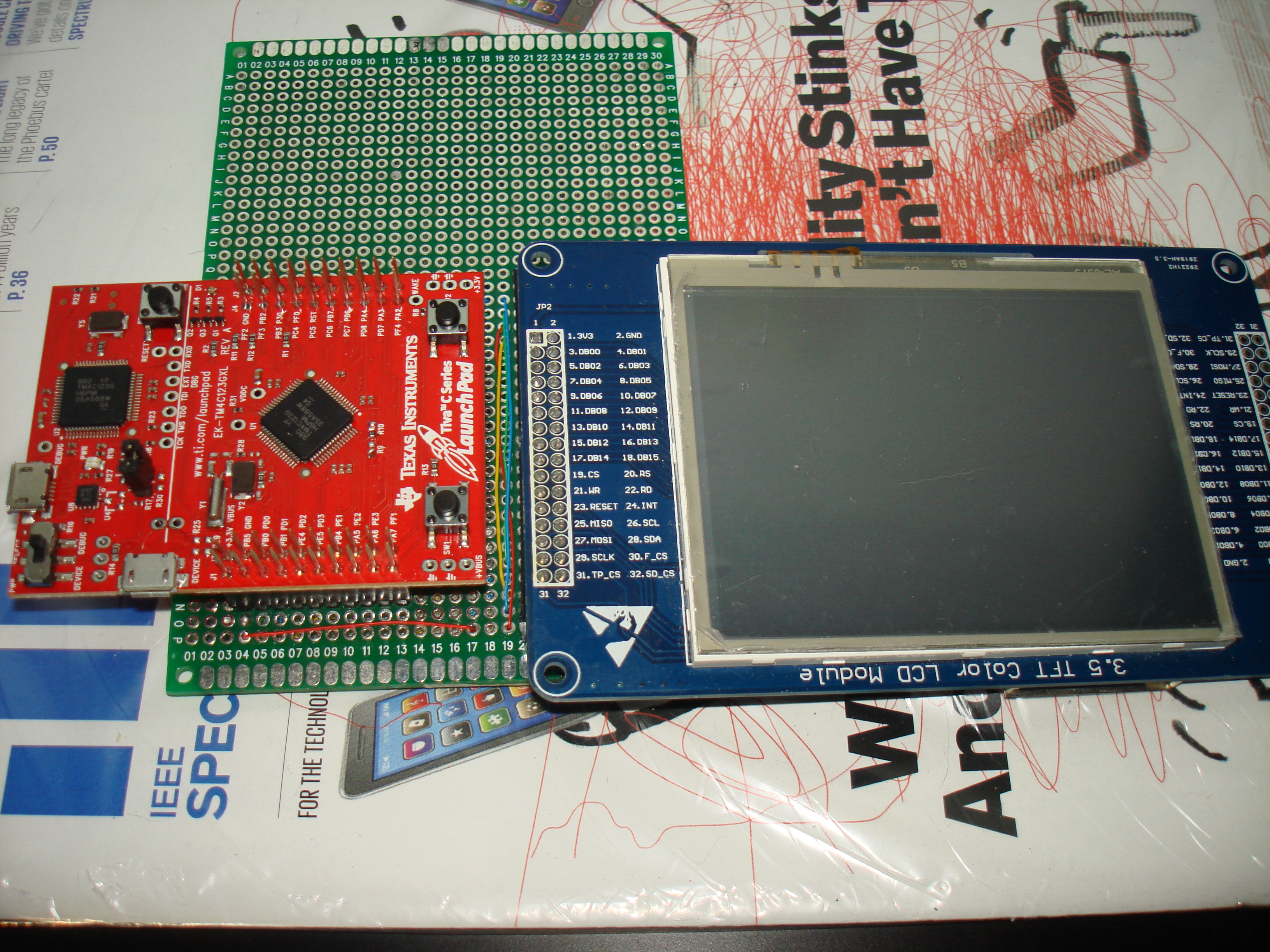
From kentec get datasheet then see where is D7 on BP connector, J2_6 PB7, D6 on J2_7 PB6, D5 on J1_2 PB5 and so on, but what is connected on EK-LM4C1294XL BP connector???
Numbering is different from schematic of Kentec and TI so transcoding show it can be on Boosterpack 2,
J1 Kentec map to TI X6 odd number J3 Kentec map to TI X6 Even number
J2 Kentec map to TI X7 Even number J4 Kentec map to TI X7 Odd number
A real disaster for a poor beginner on this so dangerous way....
J2_6,7 map to X7 12,14 PQ2, PQ3
J1_2 map to X6 3 PD2 all the other follow the port bit from new connector assignement.
And now what about all the macros shifting bits???
Bit 7 to bit 2 Destination require move 5 on right
Bit 6 to Bit 3 Destination require move 3 on right
Bit 5 to bit 2 move right 3
bit 4 to bit 0 move right 4
and bit 3 to bit 5 move left 2...
Ok the macro
#define SET_LCD_DATA(ui8Byte)
simply set all spare bit scattered over many port on 8 Bit banding...
Ok this hacking problem got solved but why not spend some word in front of this say:
Connect Boosterpack on Socket 2,
pin are assignement is different from original 120 stellaris launchpad so we adapted in this fast way...
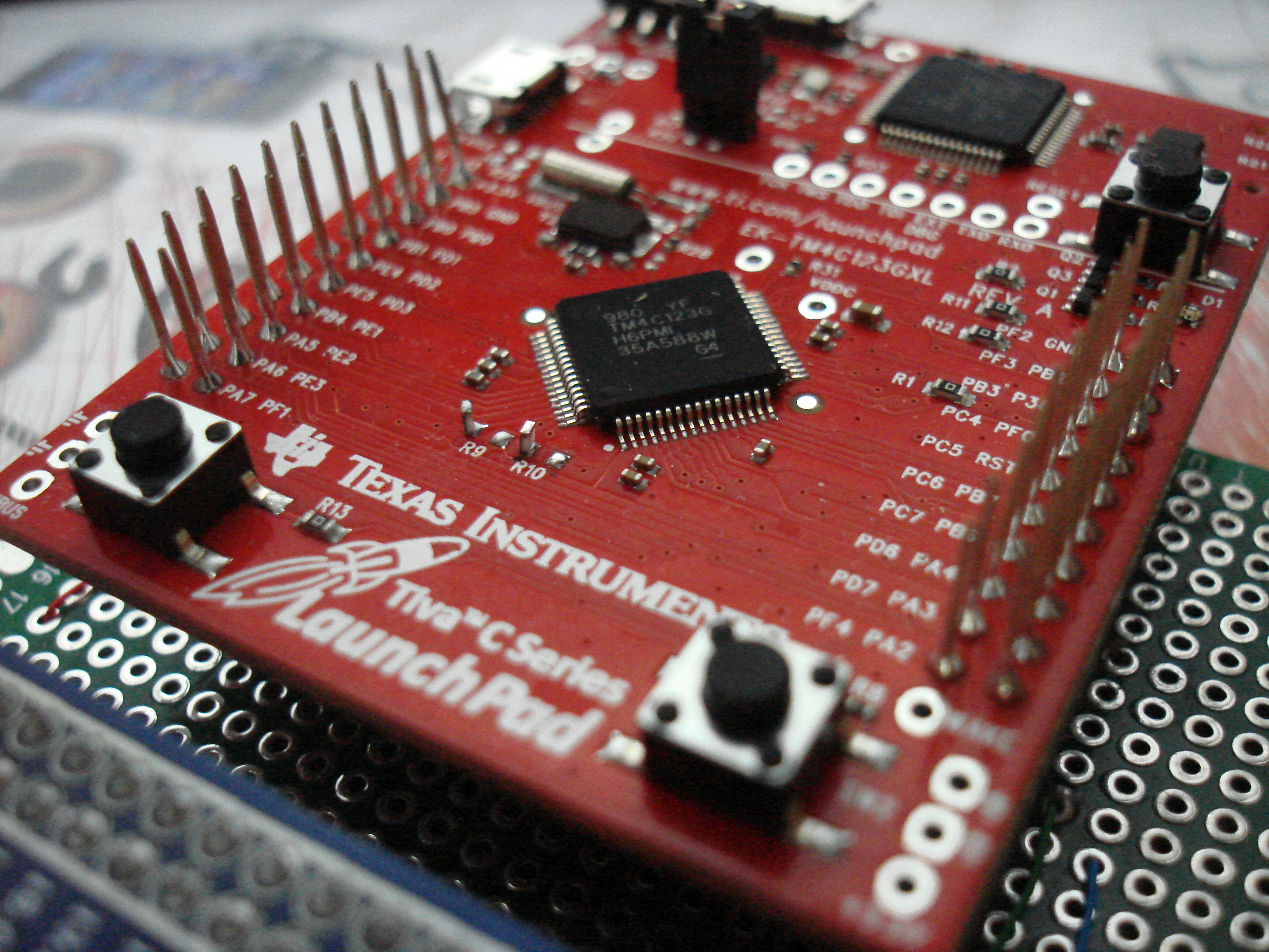
And if driver is changed a lot why not provide too a driver to use LCD BP also on 123GXL launchpad??
Data pin are on GPIO B D0 B0 ... D7 on B7
Who read this from TI please clean up all TIVAWARE library, please provide universal LCD driver usable on all example with a customization of HAL level only...
Do move on base tiwaware driver as is for Grlib too. We wish also driver for solomon and ILI simply to customize on serial or parallel interface, it is not so difficult to do.
Hey about this discover of mess up can I win something?? ;)