This thread has been locked.

If you have a related question, please click the "Ask a related question" button in the top right corner. The newly created question will be automatically linked to this question.

How to transfer the code of tiva launchpad on one single microcontroller chip?

Other Parts Discussed in Thread: TM4C123GH6PM, SEGGER

Hi,

I have a Tiva C series Launchpad with the TM4C123GH6PMI microcontroller, and I have a single TM4C123GH6PMI chip.

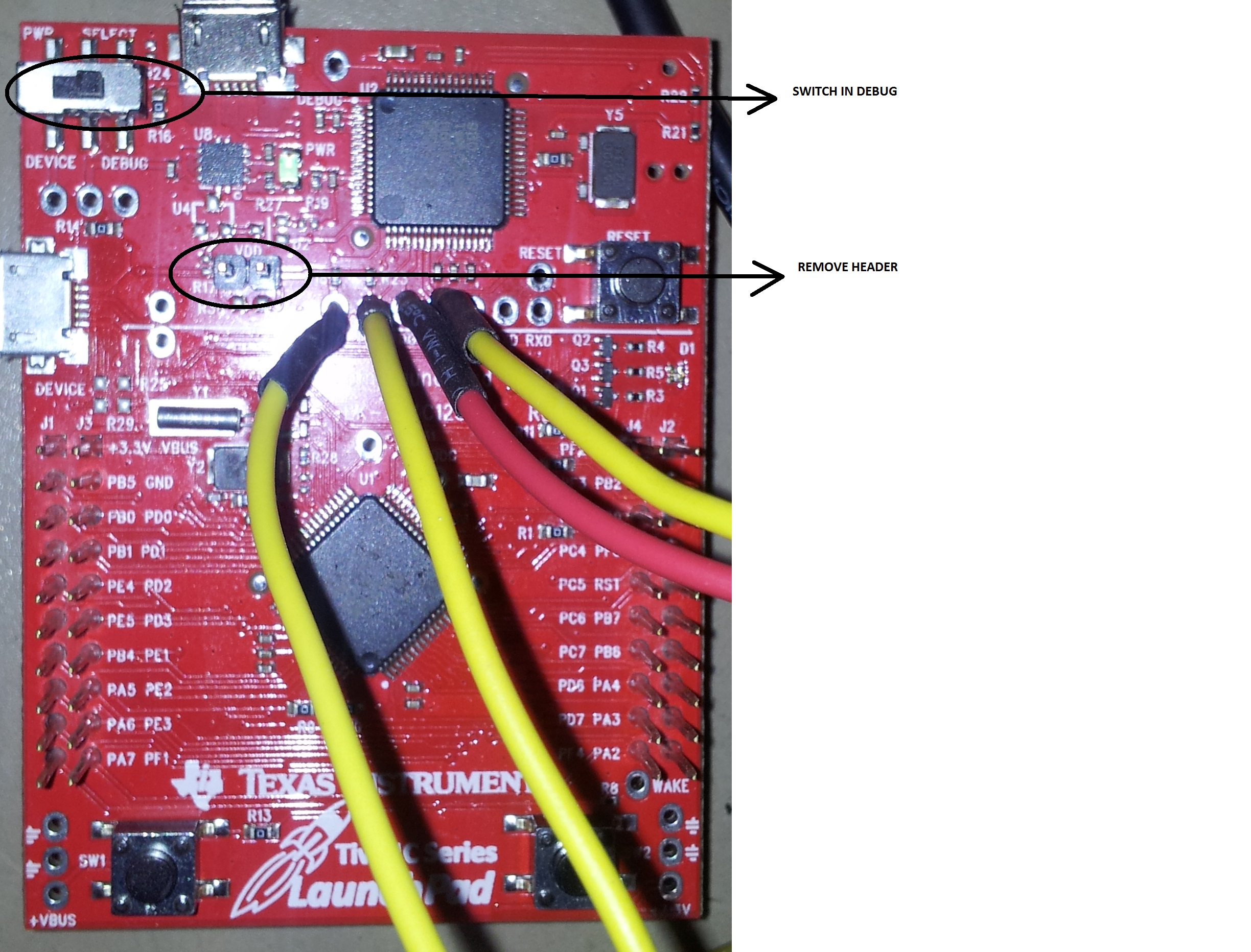
My code run very well on the launchpad, and now I would to transfer the code on the single microcontroller IC to fabricate an appropriate PCB for the my project.

How to transfer the code of tiva c series launchpad on the TM4C123GH6PMI?

I connect the debug pins of Lunchpad with the debug pins of TM4C123, or I have need to buy a jtag kit?

Thanks,

Antonino

  •  Hi, you can use an external JTAG debugger or simply use your launchpad as JTAG adaptor, remove VCC jumper then prepare wiring from debug signal to your board.

     If you buy a connected launchpad then JTAG is available as external connection on a standard 2mm connector. You need a cable adaptor or use (as I adopted like TI too [see soldering side of launchpad]) pad only programming connector, see here:

    https://www.segger.com/jlink-needle-adapter.html

    or this

    http://www.tag-connect.com/catalog/7

    or one of European distributor

    https://www.thedebugstore.com/tag-connect-push-on-pogo-pin-cables/

  • antonino proto said:
    fabricate an appropriate PCB for the my project.

    I forgot add reset <RC> network and recommended resistor to JTAG also if they are optional then take care of all capacitor in particular the one on VCCD of vcore.

  • Hello Antonio,

    You can use the Tiva-C series launchpad as a debugger as well.

    1. Keep the Switch in Debug Mode

    2. Remove the VDD Header

    3. Connect the JTAG Wires as shown in the center of the board.

    Regards

    Amit

  • Use of 4 (different) colored wires to manage that interconnect may (prevent) misconnection disaster...

  • Hello, 

    I am trying to program the TM4C123GH6PM target on a tiva-c launchpad, using a Segger j-link instead of the the debugger chip onboard the launchpad.

    The launchpad has the following pins that go from debugger to target:

    tck tms tdo tdi ext txd rxd reset

    1) Is programming is done through the the jtag port (tick tms tdo ti)? So I only need to connect these signals from the launchpad to the Segger right?

    2) Do I need to add a ground signal between the Segger and the launchpad to account for groundloop? They both connect to the same computer.

    3) Which format should I use for the compiled code? there are several options: bin/hex/out

    4) Why is txd and rxd connected to the debugger? is this for some kind of debugging?

    Thank you.

  • Hello doginwater,

    1. Yes these are the JTAG signals. However when doing so make sure that the EXT pin is connected to GND so that the on board ICDI does not interfere with the Segger J-Link
    2. Yes GND is required.
    3. You can use the Segger tools and file format supported by it.
    4. The TXD and RXD is the UART0 COM Port.

    Regards
    Amit
  • Hello Amit,

    what does EXT signal do? does it put the ICDI to sleep or something similar?
    why is UART0 connected to the ICDI?
  • Hello doginwater

    The EXT signal is to inform the ICDI that an external debugger is connected and the debugger needs to tristate its lines. I am not sure if the ICDI is put to sleep function. The ICDI MCU works as a composite device, providing a bulk class and a CDC class device to the PC Host. It can be any UART but since the device print messages are defaulted to UART port 0, UART0 is connected to ICDI for debug message print over serial terminal.

    Regards
    Amit