This thread has been locked.

If you have a related question, please click the "Ask a related question" button in the top right corner. The newly created question will be automatically linked to this question.

Tiva dk-tm4C123G how to set up multiple UARTs

Hi Experts,

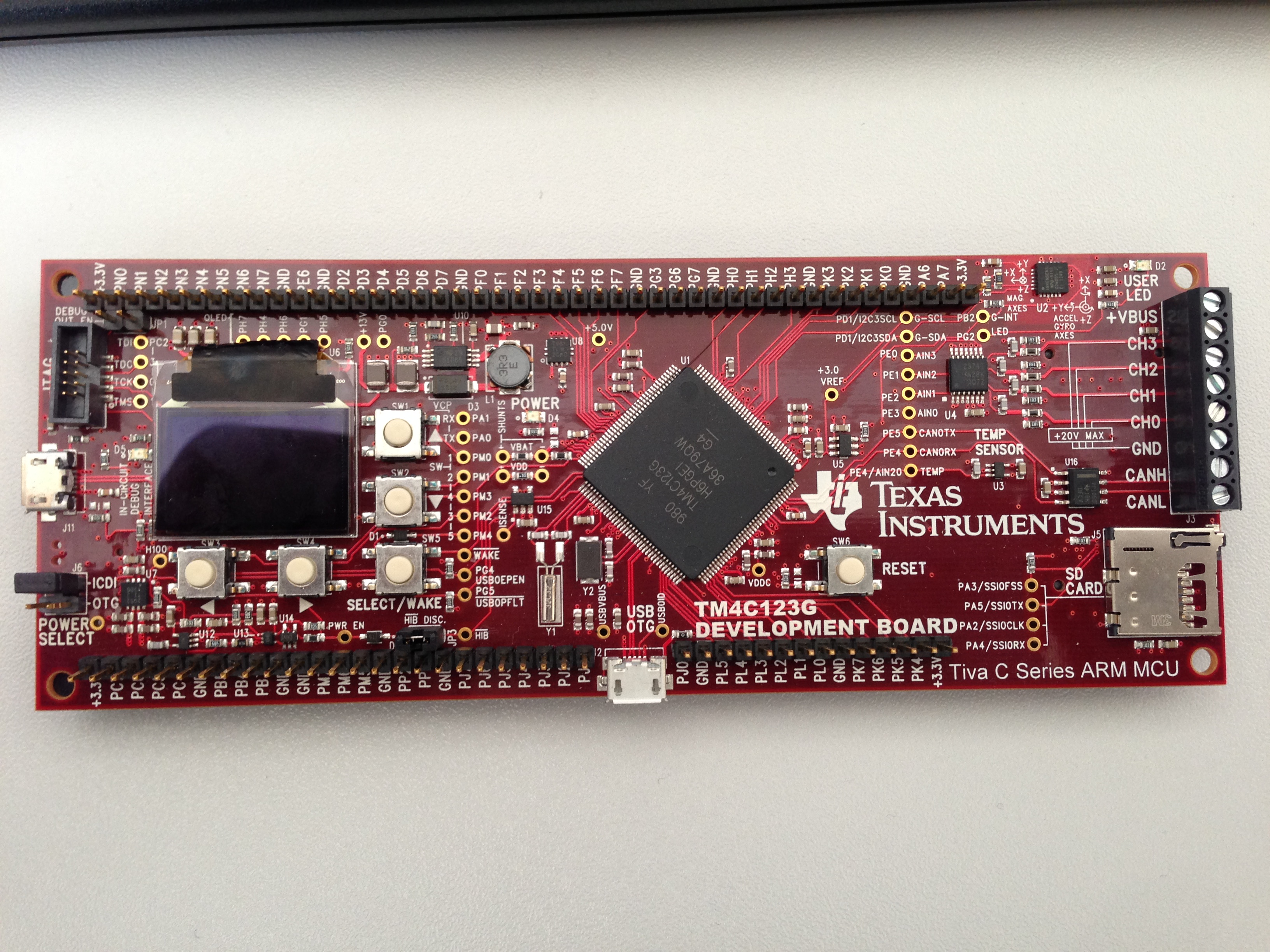
I am using the tiva dk-tm4c123g(H6PGEI36A79QWG4) board to set up multiple UARTs.

Generally speaking, the board is good with detailed output pins and easy to connect.

My question has two parts:

1. how do i setup UART2 in software level.

2. how do i have voltage for PD6(U2RX) and PD7(U2TX)?

I am eager to know why no voltage on PD6.7...

here is what I defined in source code:

#define GPIO_PORT_BASE GPIO_PORTD_BASE
#define GPIO_PIN_TX GPIO_PIN_7
#define GPIO_PIN_RX GPIO_PIN_6
#define UART_BASE UART2_BASE
#define INT_UART INT_UART2
#define SYSCTL_PERIPH_GPIO SYSCTL_PERIPH_GPIOD

I config the pins and interrupts to make UART2 to be working, maybe buggy but I leave the question later.

Currently, first step, I have to have voltage for PD6.7.

I am wondering if any "jumper" needs to be used to get voltage on pin?

Cheers,

mh

  • Hi Minghua,

    First of all, PD7 is a locked pin, please do search the forum to how to unlock it.

    Were you successful in setting up the UART1? The UART2 is exactly the same

  • Hi Luis,

    Thanks for your info.

    The reason I bypass investigating UART1 is that UART1 is used for wireless connection like Bluetooth module plugin.

    Do you think UART2 is usable as long as unlock PD7?

    Cheers,

    mh

  • Hi Minghua,

    All the UARTs in the Tiva work, they are identical. You use them as you wish, for what you want. Of course the UART1 is in most boards connected to the ICDI debugger so it's usually used to communicate with the computer serial port by USB.

    So answering your question, if you unlock PD7 you should have no problems using UART2 as you would any other UART from the Tiva

  • Hi Luis, you blog opens the gate of my problem solving.

    I think I will have more question after reading your mater-piece. :)

    Cheers,

    mh

  • Eheh, thanks.

    Master-piece? Just an attempt in having a source of information better for starters, sometimes too much info can be overwhelming so i tried to have a more simple explanations (i couldn't do professional ones anyway).

  • Btw, check this out to unlock the pins https://sites.google.com/site/luiselectronicprojects/tutorials/tiva-tutorials/note---common-errors

  • Hi Luis, thanks for your additional info.

    I read your blog and realize that the board we are using is different.

    In my case, I think I have hardware difficulty. I call it difficulty since I think the hardware is fine but there should have tricky "jumper"(hardware) or "config"(software) to activate UART2-7.

    Let me give you an example:

    If unplug the Bluetooth module(PAN1323TU) from the board, UART1(Tx. Rx) loses voltage, but if I replug the Bluetooth, UART1 works again. I think it's both sw and hw synergistic working. 

    anyone could guide me how to make those GPIO port "on power"? I think should be a easy solution but I just didnt find the entry.

    Cheers,

    mh


  • The UART1 loses voltage? Might it be that it the code used expects first a response from the bluetooth module? So that way it never transmits (and the RX lack of voltage is obvious).

    I don't see anywhere in the board configuration jumpers.

    Have you tried unlocking the pins just after enabling their GPIO clock (after a 9 cycle delay of course)

    Note that although the board is different, the MCU is about the same (both MCUs are TM4C123 series). If you check your datasheet you have PD7 and PF0 locked too.

  • Hi experts,

    I think I can do things in parallel. On one hand, I seek answer to solve my hardware voltage issue, on the other hand, I would like to discuss with you guys about the coding I made. I list some key parts of the code:

    #define GPIO_PORT_BASE GPIO_PORTD_BASE
    #define GPIO_PIN_TX GPIO_PIN_7
    #define GPIO_PIN_RX GPIO_PIN_6
    #define UART_BASE UART2_BASE
    #define INT_UART INT_UART2
    #define SYSCTL_PERIPH_GPIO_A SYSCTL_PERIPH_GPIOA
    #define SYSCTL_PERIPH_GPIO_D SYSCTL_PERIPH_GPIOD
    #define SYSCTL_PERIPH_UART SYSCTL_PERIPH_UART2
    #define RCGCUART (SYSCTL_BASE + 0x618)
    #define RCGCGPIO (SYSCTL_BASE + 0x608)
    #define GPIO_D_AFSEL (GPIO_PORTD_AHB_BASE + 0x420)

    ROM_FPULazyStackingEnable();

    ROM_SysCtlClockSet(SYSCTL_SYSDIV_1 | SYSCTL_USE_OSC | SYSCTL_OSC_MAIN |
    SYSCTL_XTAL_16MHZ);

    ROM_SysCtlPeripheralEnable(SYSCTL_PERIPH_GPIO_A);
    ROM_SysCtlPeripheralEnable(SYSCTL_PERIPH_GPIO_D);

    GPIOPinConfigure(GPIO_PD6_U2RX);
    GPIOPinConfigure(GPIO_PD7_U2TX);

    //
    // Unlock PD7
    //
    HWREG(GPIO_PORTD_BASE + GPIO_O_LOCK) = GPIO_LOCK_KEY;
    HWREG(GPIO_PORTD_BASE + GPIO_O_CR) |= 0x01;

    //
    // Choose UART2
    //
    HWREG(RCGCUART) = 0x00|0x01|0x02; //uart0, uart1, uart2
    {
    uint32_t ui32RCGCGPIO = HWREG(RCGCGPIO);
    HWREG(RCGCGPIO) |= 0x03; //GPIOD
    }

    //
    // alternate function select 1(1~8)
    //
    {
    uint32_t ui32AFSELGPIO = HWREG(GPIO_D_AFSEL);
    HWREG(GPIO_D_AFSEL) &= 0x00;
    }

    //
    // GPIODR2R (tbd)  needs to be done???
    //

    //
    // GPIOPCTL(tbd) needs to be done???
    //

    ROM_IntMasterEnable();

    ROM_SysCtlPeripheralEnable(SYSCTL_PERIPH_UART);

    ROM_GPIOPinTypeUART(GPIO_PORT_BASE, GPIO_PIN_TX | GPIO_PIN_RX);

    ROM_UARTConfigSetExpClk(UART_BASE, ROM_SysCtlClockGet(), 115200,
    (UART_CONFIG_WLEN_8 | UART_CONFIG_STOP_ONE |
    UART_CONFIG_PAR_NONE));

    ROM_IntEnable(INT_UART);

    ROM_UARTIntEnable(UART_BASE, UART_INT_RX | UART_INT_RT);

    That's all for the UART prerequisites. Enough?

    Cheers,

    mh

  • Hi Luis, good evening! Where are you? US? I saw we have big time zone difference. I am in China.

    "9 cycle delay", any reason at behind? I pasted my code but without delay parts.

    I searched PD7 and PF0 in the sheet, the only content I found out is:

    5.2.3.1 NMI Pin
    The NMI signal is an alternate function for either GPIO port pin PD7 or PF0. The alternate function
    must be enabled in the GPIO for the signal to be used as an interrupt, as described in
    “General-Purpose Input/Outputs (GPIOs)” on page 661. Note that enabling the NMI alternate function
    requires the use of the GPIO lock and commit function just like the GPIO port pins associated with
    JTAG/SWD functionality, see page 703. The active sense of the NMI signal is High; asserting the
    enabled NMI signal above VIH initiates the NMI interrupt sequence.

    I attached the doc...

    6735.Datasheet-TM4C123GH6PGE.pdf

    btw, do you have multimeter? so you can measure the GPIO(i.e., Tx of UART2,UART3... has proper voltage)?

    Cheers,

    mh

  • Hello Minghua,

    Couple of pointers here in the code from your post.

    GPIOPinConfigure(GPIO_PD6_U2RX);
    GPIOPinConfigure(GPIO_PD7_U2TX);

    //
    // Unlock PD7
    //
    HWREG(GPIO_PORTD_BASE + GPIO_O_LOCK) = GPIO_LOCK_KEY;
    HWREG(GPIO_PORTD_BASE + GPIO_O_CR) |= 0x01;

    1. The GPIO needs to be unlocked first and then GPIOPinConfigure function called

    2. The GPIO to be unlocked is PD7, whereas your code is unlocking Pin-0 or PD0. You may want to review the changes.

    Regards

    Amit

  • Hi Amit, thanks for your suggestion. I modified the code a little bit. Is it correct now?

    Regarding the voltage, still no luck. 

    I  am eager to have some new input to fix the issue. Thanks in advance!

    Cheers,

    mh

    =================================================================

    #define GPIO_PORT_BASE GPIO_PORTD_BASE
    #define GPIO_PIN_TX GPIO_PIN_7
    #define GPIO_PIN_RX GPIO_PIN_6
    #define UART_BASE UART2_BASE
    #define INT_UART INT_UART2
    #define SYSCTL_PERIPH_GPIO_A SYSCTL_PERIPH_GPIOA
    #define SYSCTL_PERIPH_GPIO_D SYSCTL_PERIPH_GPIOD
    #define SYSCTL_PERIPH_UART SYSCTL_PERIPH_UART2
    #define RCGCUART (SYSCTL_BASE + 0x618)
    #define RCGCGPIO (SYSCTL_BASE + 0x608)
    #define GPIO_D_AFSEL (GPIO_PORTD_AHB_BASE + 0x420)

    ROM_FPULazyStackingEnable();

    ROM_SysCtlClockSet(SYSCTL_SYSDIV_1 | SYSCTL_USE_OSC | SYSCTL_OSC_MAIN |
    SYSCTL_XTAL_16MHZ);

    ROM_SysCtlPeripheralEnable(SYSCTL_PERIPH_GPIO_A);
    ROM_SysCtlPeripheralEnable(SYSCTL_PERIPH_GPIO_D);

    //
    // Unlock PD7
    //
    HWREG(GPIO_PORTD_BASE + GPIO_O_LOCK) = GPIO_LOCK_KEY;
    HWREG(GPIO_PORTD_BASE + GPIO_O_CR) |= 0xFF;

    GPIOPinConfigure(GPIO_PD6_U2RX);
    GPIOPinConfigure(GPIO_PD7_U2TX);

    //
    // Choose UART2
    //
    HWREG(RCGCUART) = 0x00|0x01|0x02; //uart0, uart1, uart2
    {
    uint32_t ui32RCGCGPIO = HWREG(RCGCGPIO);
    HWREG(RCGCGPIO) |= 0x03; //GPIOD
    }

    //
    // alternate function select 1(1~8)
    //
    {
    uint32_t ui32AFSELGPIO = HWREG(GPIO_D_AFSEL);
    HWREG(GPIO_D_AFSEL) &= 0x00;
    }

    //
    // GPIODR2R (tbd)  needs to be done???
    //

    //
    // GPIOPCTL(tbd) needs to be done???
    //

    ROM_IntMasterEnable();

    ROM_SysCtlPeripheralEnable(SYSCTL_PERIPH_UART);

    ROM_GPIOPinTypeUART(GPIO_PORT_BASE, GPIO_PIN_TX | GPIO_PIN_RX);

    ROM_UARTConfigSetExpClk(UART_BASE, ROM_SysCtlClockGet(), 115200,
    (UART_CONFIG_WLEN_8 | UART_CONFIG_STOP_ONE |
    UART_CONFIG_PAR_NONE));

    ROM_IntEnable(INT_UART);

    ROM_UARTIntEnable(UART_BASE, UART_INT_RX | UART_INT_RT);

  • Hello Mh,

    And why is the AFSEL being cleared for the Port-D Pins? This is incorrect. They must be set,

    uint32_t ui32AFSELGPIO = HWREG(GPIO_D_AFSEL);
    HWREG(GPIO_D_AFSEL) &= 0x00;

    You can instead use

    GPIOPinTypeUART(GPIO_PORTD_BASE, GPIO_PIN_6 | GPIO_PIN_7);

    Regards

    Amit

  • Hi Amit,

    I think your suggestion again makes effect.

    I commented the AFSEL related out and finally I have the pin voltage.

    I use TTL2CMOS converter and serial2USB converter to show the info on PC serial terminal.

    However, what I got from the PD6.7 is random wrong message and flooded(endless wrong message with high speed).

    I checked the baud rate was correct. btw, I only connect GND and PD6.7, usually it should be enough if I ignore CTS and RTS.

    Any clue you have?

    Cheers,

    mh

  • Hi Amit, although the erratic message is still happening, I refactor the code a little bit.

    I am wondering why people dont connect multiple peripherals on this board, then they may have the similar problems. Waste such a versatile board.

    =================================================================

    #define GPIO_PORT_BASE GPIO_PORTD_BASE
    #define GPIO_PIN_TX GPIO_PIN_7
    #define GPIO_PIN_RX GPIO_PIN_6
    #define UART_BASE UART2_BASE
    #define INT_UART INT_UART2
    #define SYSCTL_PERIPH_GPIO_A SYSCTL_PERIPH_GPIOA
    #define SYSCTL_PERIPH_GPIO_D SYSCTL_PERIPH_GPIOD
    #define SYSCTL_PERIPH_UART SYSCTL_PERIPH_UART2
    #define RCGCUART (SYSCTL_BASE + 0x618)
    #define RCGCGPIO (SYSCTL_BASE + 0x608)
    #define GPIO_D_AFSEL (GPIO_PORTD_AHB_BASE + 0x420)

    ROM_FPULazyStackingEnable();

    ROM_SysCtlClockSet(SYSCTL_SYSDIV_1 | SYSCTL_USE_OSC | SYSCTL_OSC_MAIN |
    SYSCTL_XTAL_16MHZ);

    ROM_SysCtlPeripheralEnable(SYSCTL_PERIPH_GPIO_A);
    ROM_SysCtlPeripheralEnable(SYSCTL_PERIPH_GPIO_D);

    //
    // Unlock PD7
    //
    HWREG(GPIO_PORTD_BASE + GPIO_O_LOCK) = GPIO_LOCK_KEY;
    HWREG(GPIO_PORTD_BASE + GPIO_O_CR) |= 0xFF;

    GPIOPinConfigure(GPIO_PD6_U2RX);
    GPIOPinConfigure(GPIO_PD7_U2TX);

    //
    // 1.Choose UART2
    //
    HWREG(RCGCUART) = 0x4; //uart2

    //
    // 2.RCGCGPIO choose proper runing clock
    //
    {
    uint32_t ui32RCGCGPIO = HWREG(RCGCGPIO);
    HWREG(RCGCGPIO) |= 0x8; //GPIOD
    }

    //
    // 3.GPIO Alternate Function Select
    //
    {
    uint32_t ui32AFSELGPIO = HWREG(GPIO_D_AFSEL);
    HWREG(GPIO_D_AFSEL) |= 0xC0; //PD6, PD7
    }

    //
    //  4.GPIODR2R (tbd)  needs to be done???
    //

    //
    //  5. GPIOPCTL
    //

    {
    uint32_t ui32GPIOPCTL = HWREG(GPIOPCTL);
    HWREG(GPIOPCTL) |= 0x1; //Digital function field
    }

    ROM_IntMasterEnable();

    ROM_SysCtlPeripheralEnable(SYSCTL_PERIPH_UART);

    ROM_GPIOPinTypeUART(GPIO_PORT_BASE, GPIO_PIN_TX | GPIO_PIN_RX);

    ROM_UARTConfigSetExpClk(UART_BASE, ROM_SysCtlClockGet(), 115200,
    (UART_CONFIG_WLEN_8 | UART_CONFIG_STOP_ONE |
    UART_CONFIG_PAR_NONE));

    ROM_IntEnable(INT_UART);

    ROM_UARTIntEnable(UART_BASE, UART_INT_RX | UART_INT_RT);


  • report continues:

    I really dont understand how these GPIO works.

    The last moment the UART2 transmits erratic message, after I reflash the image again. Lose voltage again.

    Even with the same source code to recompile and download image, couldnt recover...

    I think I am in a dilemma and quite confused in this topic...

    Cheers,

    mh

  • Minghua YAO said:
    9 cycle delay", any reason at behind? I pasted my code but without delay parts.

    You need at least a 3 cycle delay after enabling a peripheral clock, to access their registers. So usually a SysCtlDelay(3) for good measure is a good idea.

    I live in Portugal BTW, so yea, big difference 

  • Hello Luis

    You may be right. The delay loop is missing after a direct HWREG write to the RCGC register. A better solution would be to wait for the PRGPIO register to show if the peripheral is ready for access, instead of a delay loop.

    Regards

    Amit