This thread has been locked.

If you have a related question, please click the "Ask a related question" button in the top right corner. The newly created question will be automatically linked to this question.

Tiva ADC problem with 8 Channels

Other Parts Discussed in Thread: TM4C123AE6PM

Hi,

I am facing an issue with the Tiva TM4C123AE6PM ADC.

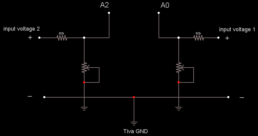
I have 8 different analog channels coming into the ADC.

Here is my configuration of the ADC and associated GPIO.

void InitGPIOD(void)
{
	// Initialise all the inputs in GPIO Port D

    GPIO_PORTD_LOCK_R = 0x4C4F434B; 	//Enable writing to GPIOCR registers
    GPIO_PORTD_CR_R = 0x000000FF;

	GPIOPinTypeGPIOInput(GPIO_PORTD_BASE, GPIO_PIN_0 | GPIO_PIN_1 | GPIO_PIN_2 | GPIO_PIN_3);

	//Initialise the above input pins as ADC inputs on the GPIO D
	GPIOPinTypeADC(GPIO_PORTD_BASE, GPIO_PIN_0);
	GPIOPinTypeADC(GPIO_PORTD_BASE, GPIO_PIN_1);
	GPIOPinTypeADC(GPIO_PORTD_BASE, GPIO_PIN_2);
	GPIOPinTypeADC(GPIO_PORTD_BASE, GPIO_PIN_3);
}
void InitGPIOE(void)
{
	// Initialise all the inputs in GPIO Port E
	// Pin 0 - MR Sensor 4 Input
	// Pin 1 - MR Sensor 3 Input
	// Pin 2 - MR Sensor 2 Input
	// Pin 3 - MR Sensor 1 Input
	// Pin 4 - 1V65 reference input
	GPIOPinTypeGPIOInput(GPIO_PORTE_BASE, GPIO_PIN_0 | GPIO_PIN_1 | GPIO_PIN_2 | GPIO_PIN_3 | GPIO_PIN_4);

	//Initialise the above input pins as ADC inputs on the GPIO D
	GPIOPinTypeADC(GPIO_PORTE_BASE, GPIO_PIN_0);
	GPIOPinTypeADC(GPIO_PORTE_BASE, GPIO_PIN_1);
	GPIOPinTypeADC(GPIO_PORTE_BASE, GPIO_PIN_2);
	GPIOPinTypeADC(GPIO_PORTE_BASE, GPIO_PIN_3);
	GPIOPinTypeADC(GPIO_PORTE_BASE, GPIO_PIN_4);
}
void InitADC(void)
{
	// Enable the clock to the ADC 0 peripheral
	SysCtlPeripheralEnable(SYSCTL_PERIPH_ADC0);
	SysCtlDelay(10);

	// COnfigure the ADC to use the internal oscillator for clocking
	ADCClockConfigSet(ADC0_BASE, ADC_CLOCK_SRC_PIOSC | ADC_CLOCK_RATE_FULL, 64);

	// Set the reference of the ADC to 3V
	ADCReferenceSet(ADC0_BASE, ADC_REF_EXT_3V);

	// Enable hardware oversampling for the ADC to increase accuracy
//	ADCHardwareOversampleConfigure(ADC0_BASE, 1);

	// Now start configuration of Sequence 0 to Read all the 8 MR sensors in one conversion
	// Disable the sequence first
	ADCSequenceDisable(ADC0_BASE, SQNC_0);

	// Configure the sequence to run at a processor trigger with the highest priority
	ADCSequenceConfigure(ADC0_BASE, SQNC_0, ADC_TRIGGER_PROCESSOR, PRIORITY_1);

	// Now configure all the steps of the sequencer to read from different channels
	// For the last channel, enable the interrupt for the channel and tell the ADC to end conversion
	ADCSequenceStepConfigure(ADC0_BASE, SQNC_0, STEP_0, ADC_CTL_CH0);
	ADCSequenceStepConfigure(ADC0_BASE, SQNC_0, STEP_1, ADC_CTL_CH1);
	ADCSequenceStepConfigure(ADC0_BASE, SQNC_0, STEP_2, ADC_CTL_CH2);
	ADCSequenceStepConfigure(ADC0_BASE, SQNC_0, STEP_3, ADC_CTL_CH3 );
	ADCSequenceStepConfigure(ADC0_BASE, SQNC_0, STEP_4, ADC_CTL_CH4);
	ADCSequenceStepConfigure(ADC0_BASE, SQNC_0, STEP_5, ADC_CTL_CH5);
	ADCSequenceStepConfigure(ADC0_BASE, SQNC_0, STEP_6, ADC_CTL_CH6);
	ADCSequenceStepConfigure(ADC0_BASE, SQNC_0, STEP_7, ADC_CTL_CH7 | ADC_CTL_IE | ADC_CTL_END);

	// Enable conversion complete interrupt for the ADC
	ADCIntEnable(ADC0_BASE, SQNC_0);
	ADCIntRegister(ADC0_BASE, SQNC_0, ISR_ADC);

	// Finally Enable the sequence
	ADCSequenceEnable(ADC0_BASE, SQNC_0);
}

Then I have the following ISR for the ADC.

void ISR_ADC(void)
{
	ADC0_ISC_R |= 0x01; //write one to clear the interrupt
	g_stApolloParms.m_etConversionStatusMR = COMPLETE;
}

The ADC is triggered in the while 1 loop.

	while(1)
	{
		static U32 ulProcessStart = RESET;
		ADC_PARMS *stADC_Parms = &(g_stApolloParms.m_stADC_Parms);

		if(ulProcessStart == RESET)
		{
			ulProcessStart = SET;
			ADCProcessorTrigger(ADC0_BASE, SQNC_0);
		}
		else
		{
			if(g_stApolloParms.m_etConversionStatusMR == COMPLETE)
			{
				g_stApolloParms.m_etConversionStatusMR = INCOMPLETE;
				ulProcessStart = RESET;
				ADCSequenceDataGet(ADC0_BASE, SQNC_0, stADC_Parms->m_ulADC_RawValue);
			}
		}
	}

Following is what happens. 

All ADC channels except channel 2 are at 0V. Channel 2 is at 1.2V (approx).

Conversion 1:

Conversion 2:

And so on...

The 1455 value is correct. The values above 4000 are certainly not correct.

The 1455 value is on channel 2. It flows into any channel. Also the other values randomly change the channels. What am I missing here, or doing something wrong?

Thanks in advance!

Makarand Deshmukh

  • Just an update, the channels on PORTD are reading 4090 and above (3v3). Please advise.
  • Hello Makarand

    Please remove the following from the configuration of the GPIO's.

    GPIOPinTypeGPIOInput

    Also PE4 is AIN9 and since you are using AIN00 to AIN07 as the channels, the configuration of this pin is not required.

    Regards
    Amit
  • Hi Amit, 

    I tried doing that earlier but with no luck. 

    Can you tell me why are the PORTD inputs reading 4095?

    The PE4 pin is required in my application (not for the purpose of this part). I intend to use another sample sequencer for that channel.

    Regards, 

    Makarand

  • Hello Makarand

    Did you try connecting Port D Pins to GND and then seeing the same?

    Regards
    Amit
  • Hi Amit, 

    Yes I did try that. They still read 4095. Suspect the internall pullup probably.

    BR, 

    Makarand

  • Hello Makarand

    The internal Pull Up's are disabled by default and I do not see that your code has enabled it. In the debugger check the value of the GPIOPUR register for Port-D.

    Also if the pin is connected to GND then the PUR will be over-ridden

    Regards
    Amit
  • Any progress? I'm facing exactly the same problem with TM4C1294NCPTD
  • Hello Kacper,

    Never heard back from the forum poster. Could you please explain the code and hw configuration you have?

    Regards
    Amit
  • Hi,

    I had actually forgotten about this post.

    I do not know if this is the correct solution but here's the scenario.

    My custom board uses a TM4C123AE6PM controller. While developing my application I was using the Stellaris EK-LM4F232 eval board.

    The code runs correctly on the custom board. 

    void InitGPIOD(void)
    {
        GPIO_PORTD_LOCK_R = 0x4C4F434B;  //Enable writing to GPIOCR registers
        GPIO_PORTD_CR_R = 0x000000FF;
    
        GPIOPinTypeGPIOInput(GPIO_PORTD_BASE, GPIO_PIN_0 | GPIO_PIN_1 | GPIO_PIN_2 | GPIO_PIN_3);
    
        //Initialise the above input pins as ADC inputs on the GPIO D
        GPIOPinTypeADC(GPIO_PORTD_BASE, GPIO_PIN_0);
        GPIOPinTypeADC(GPIO_PORTD_BASE, GPIO_PIN_1);
        GPIOPinTypeADC(GPIO_PORTD_BASE, GPIO_PIN_2);
        GPIOPinTypeADC(GPIO_PORTD_BASE, GPIO_PIN_3);
    }
    

    void InitGPIOE(void)
    {
        // Pin 4 - 1V65 reference input
        GPIOPinTypeGPIOInput(GPIO_PORTE_BASE, GPIO_PIN_0 | GPIO_PIN_1 | GPIO_PIN_2 | GPIO_PIN_3 | GPIO_PIN_4 |      GPIO_PIN_5);

        //Initialise the above input pins as ADC inputs on the GPIO D
        GPIOPinTypeADC(GPIO_PORTE_BASE, GPIO_PIN_0);
        GPIOPinTypeADC(GPIO_PORTE_BASE, GPIO_PIN_1);
        GPIOPinTypeADC(GPIO_PORTE_BASE, GPIO_PIN_2);
        GPIOPinTypeADC(GPIO_PORTE_BASE, GPIO_PIN_3);
        GPIOPinTypeADC(GPIO_PORTE_BASE, GPIO_PIN_4);
    }

    void InitADC(void)
    {
    // Enable the clock to the ADC 0 peripheral
    SysCtlPeripheralEnable(SYSCTL_PERIPH_ADC0);
    SysCtlDelay(10);

    // COnfigure the ADC to use the internal oscillator for clocking
    ADCClockConfigSet(ADC0_BASE, ADC_CLOCK_SRC_PIOSC | ADC_CLOCK_RATE_FULL, 1);

    // Set the reference of the ADC to 3V
    ADCReferenceSet(ADC0_BASE, ADC_REF_EXT_3V);

    // Enable hardware oversampling for the ADC to increase accuracy
    ADCHardwareOversampleConfigure(ADC0_BASE, 64);

    // Disable the sequence first
    ADCSequenceDisable(ADC0_BASE, SQNC_0);

    // Configure the sequence to run at a processor trigger with the highest priority
    ADCSequenceConfigure(ADC0_BASE, SQNC_0, ADC_TRIGGER_PROCESSOR, PRIORITY_1);

    // Now configure all the steps of the sequencer to read from different channels
    // For the last channel, enable the interrupt for the channel and tell the ADC to end conversion
    ADCSequenceStepConfigure(ADC0_BASE, SQNC_0, STEP_0, ADC_CTL_CH7);
    ADCSequenceStepConfigure(ADC0_BASE, SQNC_0, STEP_1, ADC_CTL_CH6);
    ADCSequenceStepConfigure(ADC0_BASE, SQNC_0, STEP_2, ADC_CTL_CH5);
    ADCSequenceStepConfigure(ADC0_BASE, SQNC_0, STEP_3, ADC_CTL_CH4);
    ADCSequenceStepConfigure(ADC0_BASE, SQNC_0, STEP_4, ADC_CTL_CH3);
    ADCSequenceStepConfigure(ADC0_BASE, SQNC_0, STEP_5, ADC_CTL_CH2);
    ADCSequenceStepConfigure(ADC0_BASE, SQNC_0, STEP_6, ADC_CTL_CH1);
    ADCSequenceStepConfigure(ADC0_BASE, SQNC_0, STEP_7, ADC_CTL_CH0 | ADC_CTL_IE | ADC_CTL_END);

    // Enable conversion complete interrupt for the ADC
    ADCIntEnable(ADC0_BASE, SQNC_0);
    ADCIntRegister(ADC0_BASE, SQNC_0, ISR_ADC);

    // Finally Enable the sequence
    ADCSequenceEnable(ADC0_BASE, SQNC_0);

    // Using the earlier method configure the other sequencer to read from the internal
    // temperature sensor in the Tiva microcontroller
    // We are using sequence 1 for this reading
    // Hardware over sampling applies to all the sequences in ADC 0, so there's no need to change that setting
    ADCSequenceDisable(ADC0_BASE, SQNC_1);
    ADCSequenceConfigure(ADC0_BASE, SQNC_1, ADC_TRIGGER_PROCESSOR, PRIORITY_2);
    ADCSequenceStepConfigure(ADC0_BASE, SQNC_1, STEP_0, ADC_CTL_TS);
    ADCSequenceStepConfigure(ADC0_BASE, SQNC_1, STEP_1, ADC_CTL_TS);
    ADCSequenceStepConfigure(ADC0_BASE, SQNC_1, STEP_2, ADC_CTL_TS);
    ADCSequenceStepConfigure(ADC0_BASE, SQNC_1, STEP_3, ADC_CTL_TS | ADC_CTL_IE | ADC_CTL_END);
    ADCIntEnable(ADC0_BASE, SQNC_1);
    ADCIntRegister(ADC0_BASE, SQNC_1, ISR_ADC_Temp);
    ADCSequenceEnable(ADC0_BASE, SQNC_1);

    // This sequence is for calculating the offset voltage
    ADCSequenceDisable(ADC0_BASE, SQNC_2);
    ADCSequenceConfigure(ADC0_BASE, SQNC_2, ADC_TRIGGER_PROCESSOR, PRIORITY_3);
    ADCSequenceStepConfigure(ADC0_BASE, SQNC_2, STEP_0, ADC_CTL_CH9);
    ADCSequenceStepConfigure(ADC0_BASE, SQNC_2, STEP_1, ADC_CTL_CH9 | ADC_CTL_IE | ADC_CTL_END);

    ADCIntEnable(ADC0_BASE, SQNC_2);
    ADCIntRegister(ADC0_BASE, SQNC_2, ISR_ADC_Reference);
    ADCSequenceEnable(ADC0_BASE, SQNC_2);

    }

  • HI,

    I use TIVA  TM4C1294XL launchpad as a multichannel voltometer with sending data through UDP protocol and displaying on LCD. Problem was very similar to that one described by Makarand Deshmukh

    I use simple voltage divider. Diagram below shows circuit.

    When I connected input voltage 1 (5.3V) (number 2 was disconnected) result  was OK ( Voltage 1: 5.3V  ;  Voltage 2 :0.0V )

    When I connected input voltage 2 (5.3V) (number 1 was disconnected) result  was only partialy OK ( Voltage 1: 0.53V  ;  Voltage 2 :5.3V )

    When I connected both inputs (5.3V) result  even more strange ( Voltage 1: 6.02V  ;  Voltage 2 :6.03V )

    I tried to change inputs on launchpad result was the same or even worse (One input always had influence on second one)

    But Yesterday I figured out what was wrong. It is problem with computer power supply. All voltages are stable and have proper levels but it generate some noise which affect the work of ADC.

    When I connected Launchpad to my old good DELL D630 laptop... measures are very stable and one channel doesn't affect on the other. So my problem is resolved

  • Hello Markand,

    One change that I see is the divider of 1 instead of the original 64. That coupled with Hardware oversampling would be killing your application getting reads from the ADC Front End.

    Regards
    Amit