Hi there,
The TM4C129X datasheet does not state which SSI pins are MISO and MOSI - even more confusing - the pins are labelled "bi-directional" ! Sureley MOSI and MISO are unidirecitonal.
|
Pin Name |
Pin Number |
Pin Mux / Assignment |
Pin Type |
Buffer Type |
Description |
|
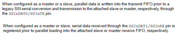
SSI0XDAT0 |
37 |
PA4 (15) |
I/O |
TTL |
SSI Module 0 Bi-directional Data Pin 0 (SSI0TX in Legacy SSI Mode) |
|
SSI0XDAT1 |
38 |
PA5 (15) |
I/O |
TTL |
SSI Module 0 Bi-directional Data Pin 1 (SSI0RX in Legacy SSI Mode) |
I’m using SSI_FRF_MOTO_MODE_2. I am connecting two TM4C129X together to communicate over SSI, One is the MASTER the other the SLAVE.
Which pin (37 or 38) is MISO and which is MOSI ?
Are the following connections correct from the TM4C129X's perspectives ?
SLAVE SSI0XDAT1 to MASTER SSI3XDAT1. This is labelled MISO on the schematic
SLAVE SSI0XDAT0 to MASTER SSI3XDAT0. This is labelled MOSI on the schematic
Our problem is that the slave is receiving all zeros but the master is outputting data as seen on a CRO.