Because of the Thanksgiving holiday in the U.S., TI E2E™ design support forum responses may be delayed from November 25 through December 2. Thank you for your patience.

This thread has been locked.

If you have a related question, please click the "Ask a related question" button in the top right corner. The newly created question will be automatically linked to this question.

Synching ADC captures with PWM at a specific cycle time

Hello everyone, I am currently developing a DC motor current controller based on the TM4C123GLX launchpad board.

I'm trying to measure the current of DC motor trough an ADC channel. The idea is to trigger ADC captures trough the PWM of the motor, each time the current crosses it's mean value. This event occurs right in the middle of the high and low semi-cycles of the PWM, therefore, I would like to trigger a capture on each semi-cycle.

example:

Period: 10 ms
duty cycle: 30%

=> ADC capture 1 at 1,5 ms after the rising edge

=> ADC capture 2 at 3.5 ms after the falling edge


I've been looking throughout the TivaWareC documentation in order to understand how does the PWM module behaves when I feed PWMGenIntTrigEnable() with one of the following trigger parameters PWM_TR_CNT_AU, PWM_TR_CNT_AD, PWM_TR_CNT_BU, PWM_TR_CNT_BD, but i couldent figure out what do they exactly do.


My question are:

- What do the previously stated configurations do?

- Should I change the load of the PWM every time I modify its duty cycle in order to trigger ADC captures at the right time with the PWM_TR_CNT_LOAD configuration? or is there a cleaner way to achieve my goal, in which a capture is performed on every semi-cycles no matter the duty cycles' value.


Thanks in advance,

Claus

  • Claus Smitt said:
    trying to measure the current of DC motor through an ADC channel

    We employ older, LX4F MCU (this vendor) to implement BLDC Motor Controller.  Our method - while not meeting all of your requirements - seems, "Good for Gov't work."

    Under StellarisWare (9453) we employ parameter, "PWM_TR_CNT_LOAD" w/in function, "PWMGenIntTrigEnable()" - and this works well for us.  (although I don't see this parameter listed in your post.)

    Also of interest/value - we employ parameter,  "PWM_GEN_MODE_UP_DOWN" w/in function, "PWMGenConfigure()."  Important to note here - is the fact that parameter "UP_Down" enables the ADC to convert at "Near center" of the PWM Cycle.  (this is especially helpful as your duty cycle shrinks - not so much as it widens...)

    We employ, "Cycle by Cycle" current-limiting - and employ the MCU's in-built PWM_Fault_Input pin to manage this - w/out software intervention - once the SW sets-up & configures the PWM Generator.  We employ the MCU's in-built analog comparator to sense currents beyond our liking - that comparator's output ties directly to our MCU's PWM Fault Input - simple & most effective.   (we note that many current spikes/transients often "self-clear" by our automatic extinguishment of the PWM drive - each time an over-current is detected by the comparator - again this w/out SW intervention!)

    Your quest for the explanation and/or operation of the (many) multiple ADC triggers you list may be read (in detail) in the Peripheral Library User's Guide - under the ADC section. 

    Question is very "far reaching" - my attempt here is to provide some (reasonable) basis to aid your experimentation...

  • Hello Claus,

    1. The configuration would generate a trigger for either the ADC or DMA when the threshold for the events are met. As an example for PWM_TR_CNT_AU when the counter in up mode crosses the GenA value a trigger is generated.
    2. To modify the DC, you would need to change the Comparator values and not the load values. Also it should not be immediate but on the next Load Count that the value should be loaded. This is controlled through the Sync register bits.

    Regards
    Amit
  • Thanks Amit and cb1 for the quick reply, thanks to your answers, I was able to find out what should to do in order to achieve my goal.

    Nevertheless, it would be very helpful that you tell me if I'm in the right track.

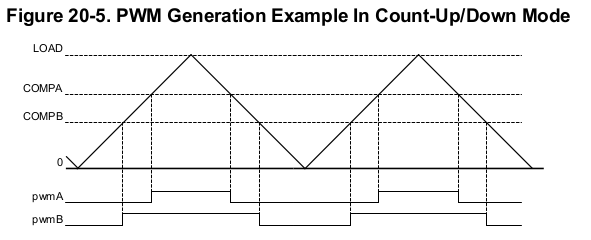
    As i saw it in the MCU's datasheet, if i configure the PWM generator in PWM_GEN_MODE_UP_DOWN mode, the 0 and LOAD event will be situated in the exact middle of the low and high semi-cycles respectively as seen in the picture.

    Therefore, I only have to configure the generator to trigger the ADC with the PWM_TR_CNT_ZERO and PWM_TR_CNT_LOAD parameters, because every time I modify the comp value with PWMPulseWidthSet() function the ZERO and LOAD events are still in the middle of each semi-cycle. Is that right?


    Thanks again,


    Regards

    Claus

    Edit: I was also wondering which is the ADC's sample & hold response time. I saw other posts related with this topic, but haven't got an accurate answer.

  • Claus Smitt said:
    configure the generator to trigger the ADC with the PWM_TR_CNT_ZERO and PWM_TR_CNT_LOAD parameters

    You move to the very "head" of this small class, Sir!  You've mastered this neat, coordinated (PWM & ADC) feature far more quickly than most.

    Like you - we were most impressed by the (unique) capability of the "Up_Down" PWM Generator configuration.  That drawing - which you nicely imported here - says it all (surely most of it) does it not?

    Believe your "ADC sample/hold" specs reveal at MCU manual end - deep in the (mostly unread) - technical/electrical specs section - under ADC...  There's little you can do there (sample/hold - unlike your earlier objective) thus you're stuck with, "what is."

    Be sure to properly mate your signal impedance to the ADC's input impedance - we (always) employ known (calibrated) voltage values so that any conversion irregularities are quickly/easily detected.  Bon chance, mon ami...

  • Hello Claus

    Yes, that is correct. However the ADC has a 4 cycle sample after which 12 cycles are spent in converting the sampled analog value. Also this is done at 16MHz, while the PWM can be working of the system clock. On top of it there is synchronization from PWM clock to ADC clock which is a value between 2-3 clocks. So if you factor in the clock ratios then the Trigger level of CompA or CompB (which is available as the other is used for PWM) may be able to give you quite an approximation

    Regards
    Amit
  • Hi Amit

    I been thinking about your answer. I can not figure out how could the delay imposed by the captures de corrected, configuring only one Comp level.

    As we said, one is fixed, and is the one that determines the duty-cycle of the control signal. therefore I only have one comp level "free" as you said. Due to the fact that the instants in which I want to perform the captures occur when the counter reaches its LOAD or 0. If I instead trigger the ADC whit one comp level, only one event can be shifted a couple of cycles, in order to perform the capture exactly at the 0 or LOAD.

    My question now is: How do shift both LOAD and 0 events to suppress the delays, with just on PWM module.


    Thanks again guys,


    Claus

  • Hello Claus

    In that case you would need to use another PWM generator which has the same Load and configuration value as the PWM generator that is being used for the actual motor operation. That way you can set the Gen A for close proximity to LOAD and Gen B for close proximity to 0, and then use the Generator triggers to sample the ADC

    Regards
    Amit
  • Hi Amit, Thanks very much! I'll start coding and testing right away.

    Regards,

    Claus
  • Hello Amit,

    I been trying to achieve what I explained in my first post throughout the day, but I can't  figure out why are the ADC interrupts not occurring.

    Sorry about the parameter redefinition, bus this is just a part of a bigger project that is currently in prototype phase.

    I set the PWM as follows:

    SysCtlPeripheralEnable(SYSCTL_PERIPH_PWM1);
    
     GPIOPinConfigure(GPIO_PD0_M1PWM0); //configurado el pin PD0 como el generador del pwm
    
     GPIOPinTypePWM(GPIO_PORTD_BASE, GPIO_PIN_0);
    
    PWMGenConfigure(PWM1_BASE, PWM_GEN_0,PWM_GEN_MODE_UP_DOWN | PWM_GEN_MODE_NO_SYNC);
    
    //Configure the ADC Triggers for current measuring
    PWMGenIntTrigEnable(PWM1_BASE,PWM_GEN_0,PWM_TR_CNT_ZERO | PWM_TR_CNT_LOAD);
    
    //Set the Period (expressed in clock ticks)
       PWMGenPeriodSet(PWM1_BASE, PWM_GEN_0, PWMModule->_PWMPeriod);
    
    // Turn on the Output pins
        PWMOutputState(PWM1_BASE, pwmBit(modNum), PWM_OUT_0_BIT);
    
        //Enable the PWM generator
        PWMGenEnable(PWM1_BASE, PWM_GEN_0);

    I set the ADC as follows:

    // enable ADC0 peripheral
        SysCtlPeripheralEnable(SYSCTL_PERIPH_ADC1);
    
        // Select the analog ADC function for these pins.
        GPIOPinTypeADC(GPIO_PORTD_BASE, GPIO_PIN_1);
    
        ADCReferenceSet(ADC1_BASE, ADC_REF_INT);
    
        IntDisable(INT_ADC1SS3);           // note we use ROM calls - yours will work as well
        ADCIntDisable(ADC1_BASE, 3);
        ADCSequenceDisable(ADC1_BASE, 3);
    
        // Enable sample sequence 3 with a processor signal trigger
        ADCSequenceConfigure(ADC1_BASE, 3, ADC_TRIGGER_PWM1, 0);
    
        // Configure step 0 on sequence 3
        ADCSequenceStepConfigure(ADC1_BASE, 3, 0, ADC_CTL_CH6 | ADC_CTL_IE | ADC_CTL_END);
    
        ADCHardwareOversampleConfigure(ADC1_BASE, 0);
    
        IntPrioritySet(INT_ADC1SS3, 3);
    
    // Since sample sequence 3 is now configured, it must be enabled.
        ADCSequenceEnable(ADC1_BASE, 3);
    
        // Clear the interrupt status flag.
        ADCIntClear(ADC1_BASE, 3);
    
        ADCIntEnable(ADC1_BASE, 3);
    
        IntEnable(INT_ADC1SS3);

    Pleas let me know if you find out where i have gone wrong in the configurations.


    Regards,

    Claus

  • Hello Claus,

    Using the debugger can you check the value of the register ADC_O_TSSEL and ADC_O_EMUX to see if for ADC1 the PWM-1 Generator 0 is selected as the source.

    Regards
    Amit
  • Amit,

    I changed from Sequence 3 to 0.

    As you asked me, I checked the registers and I got the following after the configuration is done:

    ADC_EMUX 0x00000007
    ADC_EMUX_EM3 0000-
    ADC_EMUX_EM2 0000-
    ADC_EMUX_EM1 0000-
    ADC_EMUX_EM0 0111-

    ADC_TSSELL 0x00000000
    ADC_TSSELL_PS3 00-
    ADC_TSSELL_PS2 00-
    ADC_TSSELL_PS1 00-
    ADC_TSSELL_PS0 00-

    Regards
    Claus
  • Hello Claus

    I think I understand the issue now. The following thread would be helpdul

    http://e2e.ti.com/support/microcontrollers/tiva_arm/f/908/t/376213

    Regards
    Amit
  • Hi Amit,

    After you asked me about the registers, i did exactely that, i been searching through the previous post until now.

    I added the following:

    // Configure step 0 on sequence 3
    	ADCSequenceStepConfigure(CURRENT_T_BASE, CURRENT_T_SECUENCE, 0,
    	CURRENT_T_CONFIG | ADC_TRIGGER_PWM_MOD1);
    
    	HWREG(ADC1_BASE + ADC_O_TSSEL) = ADC_TSSEL_PS0_1;

    and I got what I was expecting:

    ADC_TSSELL 0x00000000
    ADC_TSSELL_PS3 00-
    ADC_TSSELL_PS2 00-
    ADC_TSSELL_PS1 00-
    ADC_TSSELL_PS0 01-

    But the interrupt is still not happening. Could it be that I got it wrong in the Int handler or in the  int vector, I paste them below

    Code in Startup:

       IntDefaultHandler,                      // CAN0
        IntDefaultHandler,                      // CAN1
        0,                                      // Reserved
        0,                                      // Reserved
        IntDefaultHandler,                      // Hibernate
        USB0OTGModeIntHandler,                      // USB0
        IntDefaultHandler,                      // PWM Generator 3
        IntDefaultHandler,                      // uDMA Software Transfer
        IntDefaultHandler,                      // uDMA Error
        CurrentT_IntHandler,                      // ADC1 Sequence 0
        IntDefaultHandler,                      // ADC1 Sequence 1
        IntDefaultHandler,                      // ADC1 Sequence 2
        IntDefaultHandler,                      // ADC1 Sequence 3
        0,                                      // Reserved
        0,                                      // Reserved
        IntDefaultHandler,                      // GPIO Port J
        IntDefaultHandler,                      // GPIO Port K

    int Handler:

    void CurrentT_IntHandler(void) {
    
    	// Clear the ADC interrupt flag.
    	ADCIntClear(CURRENT_T_BASE, CURRENT_T_SECUENCE);
    
    	// Read ADC Value.
    	ADCSequenceDataGet(CURRENT_T_BASE, CURRENT_T_SECUENCE, &_currentBuffer[_bufferIndex]);
    
    	//increment buffer index
    	_bufferIndex++;
    
    	if (_bufferIndex >= CURRENT_T_BUFFER_SIZE){
    
    		_bufferIndex = 0;
    	}
    }

    Regards,

    Claus

  • Hello Claus,

    The interrupt should be mapped to ADC1 SS3 and not ADC1 SS0

    Also for the moment I would suggest setting the TSSEL as 0x10101010

    Regards
    Amit
  • Hi Amit,

    I am currently using sequence 0 instead of sequence 0.

    I've set TSSEL to 0x10101010 with still no interrupt triggered, do you have any thoughts on what could be happening?

    Regards,

    Claus

  • Claus Smitt said:
    I told you 2 posts ago that i changed from secuence 3 to sequence 0. 

    Perhaps you've (not yet) noted that Amit is - most always - the (only) vendor rep present here - and he can not serve you "alone!"

    Your writing (here) comes across as tad hostile and unpleasant - and is far out of proportion to the (multiple) efforts made in your behalf.

    It's in no one's interest here to attack our key vendor resource - the fast/free service you've received should be treated w/more respect & consideration...

  • I am very sorry if my previous post sounded rough, it wasn't my intention. I was just trying to clarify it... maybe I should have expressed my self in a different way. So far I'am more than greatful with the effort that you have put so far into this matter.

    Sorry again.

    Regards,

    Claus
  • Suspect that vendor's Amit appreciates your clarification.

    While my small tech firm found your post harsh - issue rises beyond expression. 

    You (and others) must realize that 20-40 new posts arrive most days - it's thus unrealistic to expect that vendor's Amit will maintain "total recall" of each/every point you raise - especially so in a long thread - as exists here.

    My writing is not directed solely to you - but as a general forum usage, "suggestion/guideline."  Posters must take great care in forming their posts - and must try to ease & prevent unnecessary, "wear/tear" upon this forum's, "Golden Goose."   

  • Hello Claus,

    Sorry for the delayed response. Unfortunately I don't have the LaunchPad handy, but what I did dig up looking at the documentation, TivaWare API and the post as well, that for PWM1 Gen0 the EMUX must have the value 0x6 and TSSEL the value 0x10 for the corresponding ADC Sequencer. Hopefully I should be able to try the same tomorrow morning.

    Hello cb1,

    Thanks for the VOC.

    Regards
    Amit
  • Hi Amit,

    Cannot stand to see (seemingly) ungrateful poster be harsh and unrealistic w/you.  I quoted (thus memorialized) {credit UCLA law} his harsh comment - which he later edited away.  

    Poster frustration is understandable - but "venom" directed toward you - uncalled for.  (w/the exceptions of my {always gentle} forum management protests!) 

    Poster's must realize that you're their, "Last, best hope" - treat w/care, kindness - and PLEASE avoid dreaded, "Does not work!"  Poster here "expected" you to have near "total recall" of his post, "changes" - that's unrealistic (you serve many here) - and surely did not justify sarcasm/harshness.  ("I told you...")  Thus - my "VOC."

    We need your great skills and "insider expertise" - newly arrived, overly demanding posters - may do well to consider forum needs (beyond) their "self-caused" frustrations... 

  • Hello Amit,

    Yesterday, After going trough the MCU's datasheet I arrived to the the same conclusion about the EMUX register. In fact I coded and debugged the following:

    // Enable sample sequence 3 with a processor signal trigger
    	ADCSequenceConfigure(CURRENT_T_BASE, CURRENT_T_SECUENCE,
    	CURRENT_T_TRIGGER, 0);
    
    	HWREG(ADC1_BASE + ADC_O_EMUX) = 0x06;

    And after the first sentence, EMUX goes directly to 0x07 that will make the ADC to expect a trigger from PWM generator 1. The second sentence is, as you said, its workaround.

    The other work around was the one you told me a couple of posts ago regarding ADC_O_TSSEL:

    // Configure step 0 on sequence 3
    	ADCSequenceStepConfigure(CURRENT_T_BASE, CURRENT_T_SECUENCE, 0,
    	CURRENT_T_CONFIG);
    
    	HWREG(ADC1_BASE + ADC_O_TSSEL) = 0x010;

    So that ADC1 sequence 0 is triggered by PWM1.


    After doing that, interrupts were generated smoothly.

    Thanks very much for all your help.

    Regards,

    Claus