


I'm implementing a reception of RS485 datagrams. The datagrams are of fixed length (9 bytes). They are received via SCI and copied to a receive buffer via DMA (block transfer). I'm observing that from time to time bytes get lost. This means sometimes only 8 bytes may get received. Since DMA always copies 9 bytes the reception gets out of sync then and DMA starts copying bytes of the next datagram. With aid of an oscilloscope I could verify that in case of a missing byte the RS485 signal was okay: the datagram on the RS485 line was complete and the signal was not noisy. The position of missing bytes is accidental. The drive enable signal for the transceiver is okay, so no bytes are cut (Rx signal was also verified).
The application is reduced to the minimum for debugging: the main task runs at only 500 Hz and there are no time consuming calculations. Nevertheless, I can observe SCI overrun interrupts from time to time. But they don't seem to be related to the cases when bytes get lost. I tried to cancel DMA and realize a pure interrupt based reception for debugging purpose. But then I got a lot of overun interrupts since the baudrate is high (1.406 MHz).
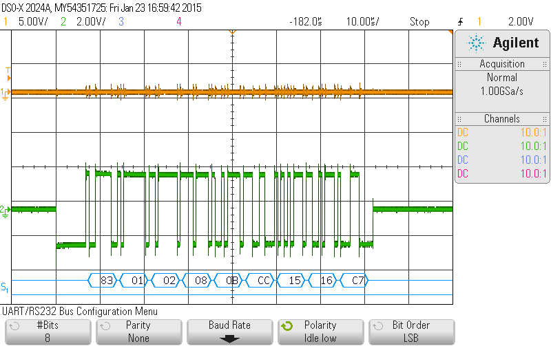
Please find attached sciInit() and dmaInit() as well as two screenshots. The screenshots show a correct datagram on the RS485 line taken with an oscilloscope and the content of the receive buffer (g_bufferedDatagram) where one byte (0x0b) is missing and the last byte 0x83 is the header of the next datagram.
Do you have any idea what the reason for this issue could be?
Thank you
Andre Niederlein

void sciInit(void)
{
/* USER CODE BEGIN (2) */
/* USER CODE END */

    /** @b initialize @b SCI */

    /** - bring SCI out of reset */
    sciREG->GCR0 = 0U;
    sciREG->GCR0 = 1U;

    /** - Disable all interrupts */
    sciREG->CLEARINT    = 0xFFFFFFFFU;
    sciREG->CLEARINTLVL = 0xFFFFFFFFU;

    /** - global control 1 */
    sciREG->GCR1 =  (uint32)((uint32)1U << 25U)  /* enable transmit */
                  | (uint32)((uint32)1U << 24U)  /* enable receive */
                  | (uint32)((uint32)1U << 5U)   /* internal clock (device has no clock pin) */
                  | (uint32)((uint32)(1U-1U) << 4U)  /* number of stop bits */
                  | (uint32)((uint32)0U << 3U)  /* even parity, otherwise odd */
                  | (uint32)((uint32)0U << 2U)  /* enable parity */
                  | (uint32)((uint32)1U << 1U);  /* asynchronous timing mode */

    /** - set baudrate */
    sciREG->BRS = 3U;  /* baudrate */

    /** - transmission length */
    sciREG->FORMAT = 8U - 1U;  /* length */

    /** - set SCI pins functional mode */
    sciREG->PIO0 = (uint32)((uint32)1U << 2U)  /* tx pin */
                 | (uint32)((uint32)1U << 1U); /* rx pin */

    /** - set SCI pins default output value */
    sciREG->PIO3 = (uint32)((uint32)0U << 2U)  /* tx pin */
                 | (uint32)((uint32)0U << 1U); /* rx pin */

    /** - set SCI pins output direction */
    sciREG->PIO1 = (uint32)((uint32)0U << 2U)  /* tx pin */
                 | (uint32)((uint32)0U << 1U); /* rx pin */

    /** - set SCI pins open drain enable */
    sciREG->PIO6 = (uint32)((uint32)0U << 2U)  /* tx pin */
                 | (uint32)((uint32)0U << 1U); /* rx pin */

    /** - set SCI pins pullup/pulldown enable */
    sciREG->PIO7 = (uint32)((uint32)0U << 2U)  /* tx pin */
                 | (uint32)((uint32)0U << 1U); /* rx pin */

    /** - set SCI pins pullup/pulldown select */
    sciREG->PIO8 = (uint32)((uint32)1U << 2U)  /* tx pin */
                 | (uint32)((uint32)1U << 1U);  /* rx pin */

    /** - set interrupt level */
    sciREG->SETINTLVL = (uint32)((uint32)0U << 26U)  /* Framing error */
                      | (uint32)((uint32)0U << 25U)  /* Overrun error */
                      | (uint32)((uint32)0U << 24U)  /* Parity error */
                      | (uint32)((uint32)0U << 9U)  /* Receive */
                      | (uint32)((uint32)0U << 8U)  /* Transmit */
                      | (uint32)((uint32)0U << 1U)  /* Wakeup */
                      | (uint32)((uint32)0U << 0U);  /* Break detect */

    /** - set interrupt enable */
    sciREG->SETINT = (uint32)((uint32)0U << 26U)  /* Framing error */
                   | (uint32)((uint32)1U << 25U)  /* Overrun error */
                   | (uint32)((uint32)0U << 24U)  /* Parity error */
                   | (uint32)((uint32)1U << 9U)  /* Receive */
                   | (uint32)((uint32)0U << 1U)  /* Wakeup */
                   | (uint32)((uint32)0U << 0U);  /* Break detect */

    /** - initialize global transfer variables */
    g_sciTransfer_t[0U].mode   = (uint32)1U << 8U;
    g_sciTransfer_t[0U].tx_length = 0U;
	g_sciTransfer_t[0U].rx_length = 0U;

    /** - Finaly start SCI */
    sciREG->GCR1 |= 0x80U;


    /** @b initialize @b SCILIN */

    /** - bring SCI out of reset */
    scilinREG->GCR0 = 0U;
    scilinREG->GCR0 = 1U;

    /** - Disable all interrupts */
    scilinREG->CLEARINT    = 0xFFFFFFFFU;
    scilinREG->CLEARINTLVL = 0xFFFFFFFFU;

    /** - global control 1 */
    scilinREG->GCR1 = (uint32)((uint32)1U << 25U)  /* enable transmit */
                    | (uint32)((uint32)1U << 24U)  /* enable receive */
                    | (uint32)((uint32)1U << 5U)   /* internal clock (device has no clock pin) */
                    | (uint32)((uint32)(2U-1U) << 4U)  /* number of stop bits */
                    | (uint32)((uint32)0U << 3U)  /* even parity, otherwise odd */
                    | (uint32)((uint32)0U << 2U)  /* enable parity */
                    | (uint32)((uint32)1U << 1U);  /* asynchronous timing mode */

    /** - set baudrate */
    scilinREG->BRS = 48U;  /* baudrate */

    /** - transmission length */
    scilinREG->FORMAT = 8U - 1U;  /* length */

    /** - set SCI pins functional mode */
    scilinREG->PIO0 = (uint32)((uint32)1U << 2U)  /* tx pin */
                    | (uint32)((uint32)1U << 1U); /* rx pin */


    /** - set SCI pins default output value */
    scilinREG->PIO3 = (uint32)((uint32)0U << 2U)  /* tx pin */
                    | (uint32)((uint32)0U << 1U); /* rx pin */


    /** - set SCI pins output direction */
    scilinREG->PIO1 = (uint32)((uint32)0U << 2U)  /* tx pin */
                    | (uint32)((uint32)0U << 1U); /* rx pin */


    /** - set SCI pins open drain enable */
    scilinREG->PIO6 = (uint32)((uint32)0U << 2U)  /* tx pin */
                    | (uint32)((uint32)0U << 1U); /* rx pin */


    /** - set SCI pins pullup/pulldown enable */
    scilinREG->PIO7 = (uint32)((uint32)0U << 2U)  /* tx pin */
                    | (uint32)((uint32)0U << 1U); /* rx pin */


    /** - set SCI pins pullup/pulldown select */
    scilinREG->PIO8 = (uint32)((uint32)1U << 2U)  /* tx pin */
                    | (uint32)((uint32)1U << 1U); /* rx pin */


    /** - set interrupt level */
    scilinREG->SETINTLVL = (uint32)((uint32)0U << 26U)  /* Framing error */
                         | (uint32)((uint32)0U << 25U)  /* Overrun error */
                         | (uint32)((uint32)0U << 24U)  /* Parity error */
                         | (uint32)((uint32)0U << 9U)  /* Receive */
                         | (uint32)((uint32)0U << 8U)  /* Transmit */
                         | (uint32)((uint32)0U << 1U)  /* Wakeup */
                         | (uint32)((uint32)0U);  /* Break detect */

    /** - set interrupt enable */
    scilinREG->SETINT = (uint32)((uint32)0U << 26U)  /* Framing error */
                      | (uint32)((uint32)0U << 25U)  /* Overrun error */
                      | (uint32)((uint32)0U << 24U)  /* Parity error */
                      | (uint32)((uint32)0U << 9U)  /* Receive */
                      | (uint32)((uint32)0U << 1U)  /* Wakeup */
                      | (uint32)((uint32)0U);  /* Break detect */

    /** - initialize global transfer variables */
    g_sciTransfer_t[1U].mode   = (uint32)0U << 8U;
    g_sciTransfer_t[1U].tx_length = 0U;
	g_sciTransfer_t[1U].rx_length = 0U;

    /** - Finaly start SCILIN */
    scilinREG->GCR1 |= 0x80U;

/* USER CODE BEGIN (3) */
   // TODO: remove for test purpose
   // Added manually, not configurable by HalCoGen
   sciREG->GCR1 &= 0xffffff7f; // get it into reset
   sciREG->SETINT |= (1 << 18); // set interrupt for RX DMA ALL
   sciREG->SETINT |= (1 << 17); // set interrupt for RX DMA
   sciREG->SETINT |= (1 << 16); // set interrupt for TX DMA
   sciREG->GCR1 |= 0x80U; // get it out of reset
/* USER CODE END */
}


void dmaInit(){

   // TX line, DMA configuration for transmission via SCI bus
   dmaReqAssign(DMA_CH0, 31); // assign request line 31 (SCI transmit) to channel 0
   dmaEnableInterrupt(DMA_CH0, BTC); // enable interrupt for block transfer complete
   // setting DMA control packets for transmit
   g_dmaCTRL dma_control_TX;
   dma_control_TX.SADD = (uint32) &g_datagramToSend; // initial source address
   dma_control_TX.DADD = ((uint32)&(sciREG->TD)) + 3; // initial destination address (big endian!)
   dma_control_TX.CHCTRL = 0; // is overwritten by some of the next commands
   dma_control_TX.FRCNT = 7U; // frame count (ITCOUNT)
   dma_control_TX.ELCNT = 1U; // element count (ITCOUNT)
   dma_control_TX.ELDOFFSET = 0U; // element destination offset
   dma_control_TX.ELSOFFSET = 0U; // element source offset
   dma_control_TX.FRDOFFSET = 0U; // frame destination offset
   dma_control_TX.FRSOFFSET = 0U; // frame source offset
   dma_control_TX.PORTASGN = 4U; // channel 0 assigned to port B (PAR0)
   dma_control_TX.RDSIZE = ACCESS_8_BIT; // read element size
   dma_control_TX.WRSIZE = ACCESS_8_BIT; // write element size
   dma_control_TX.TTYPE = FRAME_TRANSFER; // trigger type - frame/block
   dma_control_TX.ADDMODERD = ADDR_INC1; // addressing mode for source
   dma_control_TX.ADDMODEWR = ADDR_FIXED; // addressing mode for destination
   dma_control_TX.AUTOINIT = AUTOINIT_OFF; // auto-init mode
   dmaSetCtrlPacket(DMA_CH0, dma_control_TX);

   // RX line, DMA request for reception via SCI bus
   dmaReqAssign(DMA_CH1, 30); // assign request line 30 (SCI receive) to channel 1
   dmaEnableInterrupt(DMA_CH1, BTC); // enable interrupt for block transfer complete
   // setting dma control packets for transmit
   g_dmaCTRL dma_control_RX;
   dma_control_RX.SADD = ((uint32)&(sciREG->RD)) + 3; // initial source address
   dma_control_RX.DADD = (uint32) &g_bufferedDatagram; // initial destination address
   dma_control_RX.CHCTRL = 0; // next ctrl packet to be trigger + 1 (CHCTRL)
   dma_control_RX.FRCNT = 9U; // frame count
   dma_control_RX.ELCNT = 1U; // element count
   dma_control_RX.ELDOFFSET = 0U; // element destination offset
   dma_control_RX.ELSOFFSET = 0U; // element source offset
   dma_control_RX.FRDOFFSET = 0U; // frame destination offset
   dma_control_RX.FRSOFFSET = 0U; // frame source offset
   dma_control_RX.PORTASGN = 4U; // channel 1 assigned to port B (PAR0)
   dma_control_RX.RDSIZE = ACCESS_8_BIT; // read element size
   dma_control_RX.WRSIZE = ACCESS_8_BIT; // write element size
   dma_control_RX.TTYPE = FRAME_TRANSFER; // trigger type - frame/block
   dma_control_RX.ADDMODERD = ADDR_FIXED; // addressing mode for source
   dma_control_RX.ADDMODEWR = ADDR_INC1; // addressing mode for destination
   dma_control_RX.AUTOINIT = AUTOINIT_OFF; // auto-init mode
   dmaSetCtrlPacket(DMA_CH1, dma_control_RX);

   // enable channel 1 for hardware triggering
   dmaSetChEnable(DMA_CH1, DMA_HW);
   // enable DMA
   dmaEnable();
}

