


I'm trying to stack a few devices onto the TM4C123G.
I need to attach the Boostxl-Senshub, 2 SSI devices and 1 UART device.
I have the UART device on U3[PC6, PC7] and one SSI device on SSI0[PA2..PA5].
Now I'm trying to figure out where I can put the other SSI device.
SSI1[PF0..PF3] would break the LEDs connected to PF1, PF2, PF3.
SSI2[PB4..PB7] and SSI3[PD0..PD3] both seem to be blocked by the Boostxl.
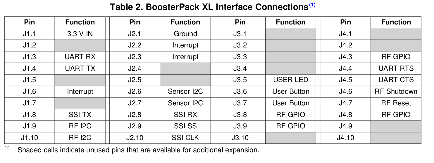
Using the examples as a guide I set up communication with the sensor hub on I2C3[PD0, PD1]. So I thought SSI2 would be open. It turns out that [PB6, PB7] are also being used for I2C communication. I monitored PD0, PD1, PB6 and PB7 with an oscilloscope and found that the same I2CSDA and I2CSCL are going through each set. The pins aren't directly connected through the Boostxl board so it appears as though the Tiva is sending commands to both sets of pins. There must be somewhere in the TivaWare code for the sensor hub that is directing the I2C commands to [PB6, PB7].
The following table indicates that [PD0, PD1] (J3.3, J3.4) are unused pins that are available for expansion and [PB6, PB7] (J2.6, J2.7) is where the I2C communication should be happening.
So what I'd really like to do is stop the talk on PD0, PD1 and make use of SSI3 (disconnecting the USER LED and User Button from the senshub).
Is anyone familiar with where the translation from PD0, PD1 to PB6, PB7 happens?

