Hello,
While I tried to understand blinky example of TM4C1220X, I got a question I could not understand.
I would appreciate it if anyone can help me understand.
in tm4c129xnczad.h file
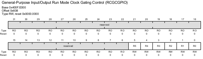
#define SYSCTL_RCGCGPIO_R (*((volatile uint32_t *)0x400FE608))
#define SYSCTL_RCGCGPIO_R14 0x00004000
in blinky.c file
int main(void)
{
volatile uint32_t ui32Loop;
//
// Enable the GPIO port that is used for the on-board LED.
//
SYSCTL_RCGCGPIO_R = SYSCTL_RCGCGPIO_R14 | SYSCTL_RCGCGPIO_R13 ;
//
// Do a dummy read to insert a few cycles after enabling the peripheral.
//
ui32Loop = SYSCTL_RCGCGPIO_R;
//
// Enable the GPIO pin for the LED (PQ7). Set the direction as output, and
// enable the GPIO pin for digital function.
//
GPIO_PORTQ_DIR_R = 0x80;
GPIO_PORTQ_DEN_R = 0x80;
......
.....
}
1. #define SYSCTL_RCGCGPIO_R (*((volatile uint32_t *)0x400FE608))
What I am understanding is this macro points to memory address 0x400FE608 which is part of peripheral bit-band region.
A value at 0x400FE608 is a single bit in the perpheral bit-band region. So the value must be 0 or 1.
The problem is SYSCTL_RCGCGPIO_R = SYSCTL_RCGCGPIO_R14
this code assigns SYSCTL_RCGCGPIO_R1 which is 0x00004000 to word in the alias region to update a single bit in the bit-band region.
I can't understand why.
2. SYSCTL_RCGCGPIO_R
Isn't this register a System Control Register? What I have known is all the system control registers are located between 0xE0000000 and 0xE00FFFFF.
are there also system control registers in SRAM and Peripheral memory regions?
Thanks for reading
Jay