This thread has been locked.

If you have a related question, please click the "Ask a related question" button in the top right corner. The newly created question will be automatically linked to this question.

ADC conversion speed issues TM4C123G

Hi all, 

I'm having an issue with a TM4C123G LaunchPad. I'm using Keil uvision 4 for programming. I'll try to make this as brief as possible:

My program has to acquire data from 3 ADC channels, process it, and send it via the UART. I use Timer 0 and systick interrupts.

Sequence is:

1) Configure every peripheral involved. 

2) Receive a specific string from UART 0 Rx channel.

3) Enable Timer 0 A, Systick and ADC Interrupts.  Systick increases a counter every 5msecs..

4) When a Timer 0 interrupt occurs, trigger an ADCProcessor conversion.

5) When a ADCInterrupt occurs (I've configured it to occur upon last conversion of the sequencer), save the ADC data in three different arrays (one for each channel), and also save the Time-stamp (i.e the Systick counter) in another array.  This way, I have a sample with its corresponding time (give or take a few cycles).

6) When X amount of adquisitions are completed, disable the interrupts, and start a routine to transfer the data via the UART 0.

The problem is, the adquisition is running VERY SLOWLY. It collects something like 15 samples in... 9 seconds!.

I believe the problem may be originated in some type of interruption-crossfire (one interrupt is triggered before another one is completed, or there is some interrupt that's taking just too much processor...)

Or perhaps I've made some mistake in this peripherals configuration. 

For the sake of clarity, I'm gonna attach here only the code regarding the ADC, Timer0 and UART configuration.

//UART 0

ROM_SysCtlPeripheralEnable(SYSCTL_PERIPH_GPIOA);

ROM_SysCtlPeripheralEnable(SYSCTL_PERIPH_UART0);

ROM_GPIOPinConfigure(GPIO_PA0_U0RX);
ROM_GPIOPinConfigure(GPIO_PA1_U0TX);
ROM_GPIOPinTypeUART(GPIO_PORTA_BASE, GPIO_PIN_0 | GPIO_PIN_1); // Configure PA0 & PA1 for UART mode.

ROM_UARTClockSourceSet(UART0_BASE, UART_CLOCK_PIOSC);   // Use 16Mhz Internal oscillator as UART clock source.

UARTStdioConfig(0, 115200, 16000000);    // Initialize UART for I/O console.
 
ROM_IntEnable(INT_UART0);
ROM_UARTIntEnable(UART0_BASE, UART_INT_RX | UART_INT_RT); // Enable Rx and Rt interruptions

//Timers & Systick

ROM_SysCtlPeripheralEnable(SYSCTL_PERIPH_TIMER0); // Timer 0, to trigger ADC adquisitions.

// Enable processor Interrupts
ROM_IntMasterEnable();

// Configure 32bits periodic timer.
ROM_TimerConfigure(TIMER0_BASE, TIMER_CFG_PERIODIC);
ROM_TimerLoadSet(TIMER0_BASE, TIMER_A, ROM_SysCtlClockGet()*3);

ROM_IntEnable(INT_TIMER0A);
ROM_TimerIntEnable(TIMER0_BASE, TIMER_TIMA_TIMEOUT);     // Configure interrupts.

//Enable Timer0
// ROM_TimerEnable(TIMER0_BASE, TIMER_A); 

// Enable Systick every 5msecs
ROM_SysTickPeriodSet(100000); // 5ms @ 20MHz
ROM_SysTickIntEnable();
ROM_SysTickEnable(); // Starts count

//ADC 

ROM_SysCtlPeripheralEnable(SYSCTL_PERIPH_ADC0);
ROM_SysCtlPeripheralEnable(SYSCTL_PERIPH_GPIOE);

ROM_GPIOPinTypeADC(GPIO_PORTE_BASE, GPIO_PIN_1 | GPIO_PIN_2 | GPIO_PIN_3);     // Configure ADC pins: PE1,PE2,PE3.

ADCSequenceDisable(ADC0_BASE, 2); //Disable Sequencer 2 before configuring.

// Configure ADC0, sequencer 2, processor trigger and priority 0 (highest).
ROM_ADCSequenceConfigure(ADC0_BASE, 2, ADC_TRIGGER_PROCESSOR, 0);

// Configure every ADC steps. Step0-Channel0,  Step1-Channel1 and so on.
ROM_ADCSequenceStepConfigure(ADC0_BASE, 2, 0, ADC_CTL_CH0 );
ROM_ADCSequenceStepConfigure(ADC0_BASE, 2, 1, ADC_CTL_CH1 );
ROM_ADCSequenceStepConfigure(ADC0_BASE, 2, 2, ADC_CTL_CH2 | ADC_CTL_IE | ADC_CTL_END); //Last sample, enable ADC interrupt.

//This way I'm certain every sample is taken when the interrupt triggers.

ROM_ADCSequenceEnable(ADC0_BASE, 2);  //Enable Sequencer 2

ROM_ADCIntClear(ADC0_BASE, 2); //Clear interrupt flag before starting.

ROM_ADCIntEnable(ADC0_BASE, 2); // Enable ADC interrupts.

Then the Interrupt Handler for the Timer0 does this:

void Timer0InterruptHandler(void)
{
ROM_TimerIntClear(TIMER0_BASE, TIMER_TIMA_TIMEOUT);   //Erase timer0 interrupt Flag

ADCProcessorTrigger(ADC0_BASE, 2);  //Trigger ADC conversion
}

And the ADC Interrupt Handler does this:

void ADCInterruptHandler(void)
{
ROM_ADCIntClear(ADC0_BASE, 2); // Erase interruption flag

// Obtain sequencer data
ROM_ADCSequenceDataGet(ADC0_BASE, 2, &SetDatosADC[0]); 

ADCInterruptIsTrue=true; // Raise a flag to process data in main loop.

}

//Then, in the Main Loop.........

if (ADCInterruptIsTrue)

TimeStamp[indice] = ContadormsegSystick;

// Process and convert every analog input channel.
ui32Millivolts = (SetDatosADC[0] * 4100) / 819; // Position AN0=PE3.
Position[index] = (int16_t)ui32Millivolts;

ui32Millivolts = (SetDatosADC[1] * 4100) / 819; // Strength AN1= PE2.
Strength [index] = (int16_t)ui32Millivolts;

ui32Millivolts = (SetDatosADC[2] * 4100) / 819; // Temperature AN2=PE1.
Temperature[index] = (int16_t)ui32Millivolts;

ADCInterruptIsTrue=false; 

index ++;

}

I've  realized I can trigger an ADCTimer conversion instead of triggering the ADCProcessor inside the Timer0 Interrupt. But,  I don't know if it makes any difference regarding execution speed. Does it?

I'm not sure if the clocks settings are correct, as they seem to be different for some peripherals (Example; the UART and the Timers).

I really appreciate any feedback on this matter.

Kind Regards.

Martin

  • Ok, I've partially solved (?) some of these issues. 

    I was unnecesarilly using an excesive value for Timer0 interrupt. I was using the 20Mhz  System clock configuration. And this statement:

    // Configure 32bits periodic timer.
    ROM_TimerConfigure(TIMER0_BASE, TIMER_CFG_PERIODIC);
    ROM_TimerLoadSet(TIMER0_BASE, TIMER_A, ROM_SysCtlClockGet()*3);

    Yielded a delay of 3*20000000 ----=    3seconds between each Timer0 interrupt.

    I've changed system clock to 40Mhz, and reduced the Timer0 Load Value to 400k:

        ROM_TimerLoadSet(TIMER0_BASE, TIMER_A, 400000);

    At 40Mhz, this yields a delay of 10msec between each Timer0 interrupt. 

    Then I've used systick interrupt, set to be triggered each 1msec.

    ROM_SysTickPeriodSet(40000); 

    Every time the ADC interrupt is called (i.e, the three conversions are complete), I also save the Systick value.

    When I finish the adquisition, I print all the results in the UART,

    What I'm seeing is that Sytick-generated "time stamps" occur every 7msec, not 10msec. Why is that?

    And, my main issue is... if I try to lower the Timer0 set value, the whole system malfunctions. (The adquisition never stops, or the data isn't processed, or even the characters printed by the UART are cut).

    Any thought on how cn I improve the ADC speed?

    Thanks for taking the time to read my post.

    Regards,

    Martin.

  • Hi Martin,

    Can you just share how exactly your configuring the clock for 40Mhz?
  • Hi, Luis

    I'm doing:

        ROM_SysCtlClockSet(SYSCTL_SYSDIV_5 | SYSCTL_USE_PLL | SYSCTL_XTAL_16MHZ |
                           SYSCTL_OSC_MAIN);

    If I use the command:  

    	  UARTprintf("Clock: %d \n",SysCtlClockGet());

    I get:

    Clock: 40000000   

    I think I find one of my problems. While testing the interrupt routines sequence, I used the UARTprintf command inside the interrupts. I believe this is what caused the timing differences between the Timer0 and the Systick interrupts. I've removed every UARTprintf from the interrupts, and now both timers match at 10msec.

    But my question still is, how can I lower the speed to 1msec, for example?

    Thanks for your response

    Martin

  • Well, I've finally managed to solve the ADC speed issue.

    Turns out it was completely related to the use of the UARTprintf command during an interruption. (It was the fastest way I could think of, for testing if the Interrupt sequence was executing in the correct order.. just printing out "Timer0 interrupt triggered" for example,  and so on)

    Now it seems to me like a quite obvious mistake. But well... this is the way one learns...

    Now I'm having a different type of problem. I'm reading from the 3 ADC channels, which I've configured in pins  PE1, PE2  and PE3.

    When I try placing a known voltage in one of the pins, the other ones (which aren't connected to anything) get affected as well.

    Could this be related to the ADC configuration?

    My code for this part is:

    ROM_SysCtlPeripheralEnable(SYSCTL_PERIPH_ADC0);
        ROM_SysCtlPeripheralEnable(SYSCTL_PERIPH_GPIOE); 
    
        // Configure input pins for the ADC.   PE1,PE2,PE3.
        ROM_GPIOPinTypeADC(GPIO_PORTE_BASE, GPIO_PIN_1 | GPIO_PIN_2 | GPIO_PIN_3);
        
       ADCSequenceDisable(ADC0_BASE, 2); //Befor configuring ADC Sequencer 2, turn it off.
    	
        ROM_ADCSequenceConfigure(ADC0_BASE, 2, ADC_TRIGGER_PROCESSOR, 0);
    	
        // Configure every step from the Sequencer 2. For each one, change tje step number and channel. Step 0-Channel 0. Step 1-Channel 1, etc. 
    		ROM_ADCSequenceStepConfigure(ADC0_BASE, 2, 0, ADC_CTL_CH0 );
    		ROM_ADCSequenceStepConfigure(ADC0_BASE, 2, 1, ADC_CTL_CH1 );
    		ROM_ADCSequenceStepConfigure(ADC0_BASE, 2, 2, ADC_CTL_CH2 | ADC_CTL_IE | ADC_CTL_END);  //Last conversion, enable ADC interrupt
    		
       	//This way I'm certain I've obtained all the data for this sample time when the ADC interruption is triggered.
    				
        // enable sequence 2
        ROM_ADCSequenceEnable(ADC0_BASE, 2);
    		
        // Erase interrupt status flag. 
        ROM_ADCIntClear(ADC0_BASE, 2);

    Then in the main loop I do:


    // Enable ADC sequencer 2
    ROM_ADCSequenceEnable(ADC0_BASE, 2);
    
    // Flush ADC sequencer.
    ROM_ADCSequenceDataGet(ADC0_BASE, 2, &SetDatosADC[0]);
    
    // Enable ADC interrupts.
    ROM_ADCIntClear(ADC0_BASE, 2);
    ROM_ADCIntEnable(ADC0_BASE, 2);

    Is there a problem with this ADC configuration?

    Thanks

    Martin

  • Martin Cunningham said:
    When I try placing a known voltage in one of the pins, the other ones (which aren't connected to anything) get affected as well.

    Just to be sure I understand.  The other pins are floating?  I.E. you have a voltage on one pin and the other pins are not connected to any voltage source or to ground?

    If so, that may be sufficient to explain your problem.  The inputs on an A/D system like on the TIVA are not fully independent.  They share sampling circuitry.  When the input is switched to a channel the source on that channel charges or discharges a sampling capacitor.  When it switches to a different channel the charge is retained and if there is nothing connected to that channel it will have essentially the same voltage as the previous channel. An oversimplification but maybe enough to get started with.

    That is why the A/Ds have a maximum source impedance specification. The source must be capable of charging and discharging that sample capacitor quickly. I typically use a capacitor on the input to provide a local low impedance source. 

    As I did earlier for another poster, I would recommend that if you get a chance attend this vendor's (or another analog vendor's) seminar on data acquisition.

    Robert

  • As usual - poster Robert & this reporter are in agreement.    Always unwise to allow an MCU input (GPIO or Analog) to simply "float."

    As Robert outlined - that shared analog input cap requires great "care/handling" to function optimally.   And - we've noted - both this vendor & other ARMs - that often there's is, "signal bleed or crosstalk" especially so upon, "successive channels" w/in your "Step Configuration."

    You can reduce this signal bleed by employing the 8 step configuration - and always including a "dead channel" (yet not floating) - between each of your desired channel conversion steps.   (the significance of the 8 step configuration - assuming you measure 4 or fewer ADC channels - is the availability of an interposed "dead channel.")    The greater the difference between signal voltage - on consecutive step channels - the larger this "bleed impact."

  • Sorry I couldn't follow up Martin, I didn't have access to a computer.

    Glad you found the problem. You can now get triggers bellow 1ms intervals? Note that the ADC requires to be configured to handle high conversion speeds. By default I think it's 125K. There isn't any function for that right now (that I know of) so you need to check the ADC register map, bit field to configure is in the ADCPP register.

    That influence you describe is perfectly normal. When left floating the pins "do whatever they want" depending on influences (so basically teens ? :p)
    For Robert and cb1 both give good suggestions to solve the situation while I ask:
    Would not the internal pull-up/down be enough for the purpose or does it have too much impedance (haven't checked)
  • Luis Afonso said:
    Would not the internal pull-up/down be enough for the (ADC) purpose

    Those pull-up/down are primarily employed when pin is "Digital" - don't believe they may be (effectively) enabled when pin is config'ed as ADC...

    And - they'd "color" your analog readings somewhat - would they not?

  • Thanks Robert, cb1- and Luis for your responses!

      That  was very informative. I'm gonna start by implementing cb1-'s suggestion of leaving a 'dead' channel in between. 

    If I understand correctly, this "dead channels" should be pulled down with an appropiate value resistor (I believe the eternally appealing 10k should do the trick, right?). 

    Luis, I think it is a very good idea to check the ADCPP register to find out the actual speed that is set. I've read the TM4C datasheet, and found this:

    ADC0 base register address is: 0x4003.8000
    ADCPP register offset is: 0xFC0

    According to what I've read, I've got to use the HWREG function to directly access this register and be able to read it.  I thought of performing a "read" on this register, and then displaying this read value using the UART.

    But how can I use it properly? I thought of using these statement, but it generates an error condition: 

    uint32_t ADCPP =HWREG(0x4003.8000+0xFC0);
    
    UARTprintf("Register value: %d",ADCPP);

    Again, thanks for taking the time to read this.

    Regards, 

    Martin

  • Hi Martin,

    About the register access. When consulting the datasheet it can be easier to use straight out values instead of macros. But not that the "." should not be there (what's 13,5? it's a float right? well it's the same)! 0x40038000 is what you should use.
    Check here for the use of that register and the macros (even thought it says stellaris)
    forum.43oh.com/.../7153-stellaris-fast-analog-reads
  • Martin Cunningham said:
    If I understand correctly, this "dead channels" should be pulled down with an appropiate value resistor (I believe the eternally appealing 10k should do the trick, right?). 

    I don't recall what chip you are using so check your documentation.  However, the one I am using specifies a maximum source impedance of 500 Ohms.  I would use a 100 Ohm or less pull down in that case.

    Robert

  • Even if enabled I doubt they'd be strong enough. Port pull-up/downs are designed for high impedance digital inputs.

    Robert
  • While (past) employed at (another) semi-giant - MCU pins which could be config'ed as Digital or Analog rarely shared internal routings and/or components.   I continue in the belief that the "digital" pull-up/down does not impact the pin when config'ed as Analog.

    To realize the least harmful impact from this noted, adjacent signal-step, "bleed" tieing the "dead channels" to V(A)/2 (i.e. 1/2 scale) may prove helpful.

    In our case - when (really) trying to squeeze every "bit" from an MCU's ADC - we may route the same signal to adjacent signal-step MCU pins - and then reject the first ADC reading.    (as its the one most impacted by such bleed - this "back to back" ADC read eliminates any "delta V" influence)    Indeed this "halves" the number of ADC channels - yet we've observed this bleed to easily add 3-4 bits of error - to the ADC's reading.

    Again - we note this effect across multiple ARM MCUs - from many makers.    Best/brightest ADCs exist here/other "Analog specialty firms" - and surely should be considered - if the truest & most repeatable/consistent analog results are important...

  • I've used micros where the pull-up was configured at the pin rather than rather than after the mux to the functional block. And of course micros with few if any internal pull-up/down functionality. I wouldn't be surprised either way. But I doubt it really matters since the pull-ups will be designed for high impedance inputs rather than analogs.

    Robert
  • Robert Adsett said:
    I've used micros where the pull-up was configured at the pin rather than rather than after the mux to the functional block.

    I'd bet those were (not) ARM MCUs!    You must keep in mind that any such "pull-up" would route to Vdd - not VdAnalog - and thus would be a rich source of (unwanted) digital switching noise.    Every ARM vendor we've noted complies w/this (prohibit the pull-up R when in analog) design goal...

  • I think one of them was actually. I don't think the vendor was suggesting the pull-up be connected when used as an analog it just wasn't prevented.

    IIRC, you could have both the GPIO and A/D hooked up at the same time. I think that was just an implementation side-effect rather than an intended use.

    Robert
  • We must disagree then. (at least w/your recall)   With confidence I can state that the ARM MCU market leader (by far) does not allow the internal, pull-up R to reach the analog input - when in analog mode.   Perhaps your (recalled) part was stripped version - pin limited - and not of the, "high-performance class."

    Note too that "serious" MCUs with ADCs (always) include separate pins for digital and analog power.   "Never the twain shall meet" (especially applicable to digital vs. analog) was - and continues to be - sound advice...    Violation of enough - commonly known/agreed design guidelines - may not serve readers well...

  • Well, I think we've got quite a debate here. =)

    Luis, I've checked your suggestion. 

    If I'm not mistaken, the following line sets the ADC in a sample rate of 1MSPS, correct?

    HWREG(ADC0_BASE+0xFC0) &= ~0xF;      // ---- Set the last 4 bits of ADCPP register in 0000.
    HWREG(ADC0_BASE+0xFC0) |= 0x7;         //  ---- Set the last 4 bits of ADCPP register in 0111.

    So, If I try the following modification:

    HWREG(ADC0_BASE+0xFC0) &= ~0xF;      // ---- Set the last 4 bits of ADCPP register in 0000.
    HWREG(ADC0_BASE+0xFC0) |= 0x5;         // ---- Set the last 4 bits of ADCPP register in 0101.

    It should change the ADC max sample rate to 500ksps.

    But how can I be sure this setting is being performed correctly?

    (Maybe I'm just stubborn, but...) I tried making the following:

    uint32_t ADCPP =HWREG(ADC0_BASE+0xFC0);
    UARTprintf("%x \n",ADCPP);

    With the two different settings (0x7 or 0x5) , the screen just printed out: "B020C7".

    Now, I know that ADCPP 32-bit register has the first 8 bits "reserved". Is this analysis correct? Does the number I'm gettting belong to the 24 non-reserved remaining bits of the ADCPP register? If that were the case, I've got a 0x7 in the 3 LSB of the register, which corresponds to 1MSPS.

    If (and only if) this reasoning was correct... that means the max sample rate isn't changing, correct?

    cb1- , Robert: Your conversation has been most informative. I'm gonna try the physical-resistor pull down approach, (I'm in no way in a state of being able to perform test with the digital pull up/downs feature. As I wouldn't know what to conclude from the results obtained. So I'm going with the long-tested "analog" resistor method (je). As soon as I have some results, I'll post them, in case they are of use to someone else.

    Many thanks for your assistance !

    Martin

  • Martin Cunningham said:
    Well, I think we've got quite a debate here. =)

    Not much of a debate really.  We're counting angels.

    We both agree that internal pull-ups are ineffective for assuring an A/D level.

    Make sure you use a low resistance pull down Martin.

    Robert

  • Dear all, 

      I've continued with this design. I'm finishing the hardware design stage. Following your recommendations, and reading the TM4C123 datasheet, I've added an Input RC circuit.  (Along with some clamping diodes to keep everything within the 0V - 3.3V range).

    According to datasheet, a source impedance of Zs=500 ohm allows for a T=250 nsec period. 

    If I'm not mistaken, 100ohm-1uF should allow a  500 usec period, i.e a 2KHz sampling rate.  (Consdering a sample-time 5 times larger than the time-constant).

    I've got the following doubt. I'm triggering an ADC reading every 500 usecs. Each reading samples the 8 channels. Then I just take the values in channels 0, 3 and 7 (this is to avoid the signal "bleeding" between adjacent channels, as  cb1- kindly suggested).

    So, the sequence should be:

    Time 0: Trigger ADC conversion

    Time ?: ADC conversion finished. Save channels 0,3,7 values. 

    Time 500 usec: Trigger another ADC conversion....          etc

    I do not know the real speed with which the ADC takes the 8 readings. THIS should be the real speed I filter with my sampling cap- resistor. Correct?

    I can't figure a correct way to measure the real ADC sampling rate, as accessing the  ADCPP register doesn't seem to work as I explained in previous post (and the SYSCTL_ADCSPEED_125KPS approach isn't an option anymore).

    I'd appreciate your feedback on this issue.

    Thanks for taking the time to read this.

    Regards.

    Martin

  • That 1µF looks high to this reporter.

    Bit of indirection - exciting a "single" ADC channel with the (properly level set) "digital" output of a frequency generator - or from your MCU's GPIO (config'ed as output) can provide, "real-world measure" of your ADC's sampling speed!

    Toggle that GPIO - and when fed (routed) to a single ADC channel - with the 8-step configuration - you will note sequential ADC readings of, "full scale & near zero" when the frequency of that GPIO toggle "near equals" your ADC's conversion rate.     We have little interest in the precise ADC values - you simply want to establish that the ADC has "recognized" the difference - between the GPIO's digital, "low and high."

    Perhaps the simplest means to achieve fine (and wide) GPIO frequency control is via one of the MCU's Timers - configured into its PWM mode.    (this is the only way I know - to secure the "escape/output" - of a "direct" timer signal.)      Normally the external Timer pin serves as Timer Input only.

    We've long used this method - both during initial "test/verify" - and "downstream" - to best insure that what we "believe" to be happening has (some) basis in reality...

  • Martin Cunningham said:
    I do not know the real speed with which the ADC takes the 8 readings. THIS should be the real speed I filter with my sampling cap- resistor. Correct?

    No.  Your R/C filter is a simple filter to remove or reduce frequencies about your sample rate (0.5 ms in your case). Strictly speaking if you you want to eliminate all frequencies above 1/2 your sample rate (See Nyquist frequency for further reading, you can get more subtle than that) but I've found a simple RC filter near the Nyquist frequency work well in many cases.  If your signal has a lot of frequencies near your sample rate you may want to revisit that assumption.

    For 2kHz sampling rate you would want a time constant of 0.5ms or longer. 1mS or longer may be preferable.

    You can add additional filtering internally to reduce the frequency further if your internal loop runs slower than your sample rate.

    Martin Cunningham said:
    I've got the following doubt. I'm triggering an ADC reading every 500 usecs. Each reading samples the 8 channels. Then I just take the values in channels 0, 3 and 7 (this is to avoid the signal "bleeding" between adjacent channels, as  cb1- kindly suggested).

    If you do that, make sure the "bleed channels" are tied to a constant value via a low impedance.

    Check that you op-amp is stable driving that load.  100Ohms is probably sufficient to keep it stable but it's worth checking. Some op-amps will be noted as capable of driving a capacitive load.

    Robert

  • Poster receives "two for the price of one" - cleverly each response covers different area! (for those keeping score - Robert's clock still "off" by 1 minute!)
  • I've continued working on this project, Thanks everyone for your collaboration, especially cb1- and Robert. You've been most helpful.

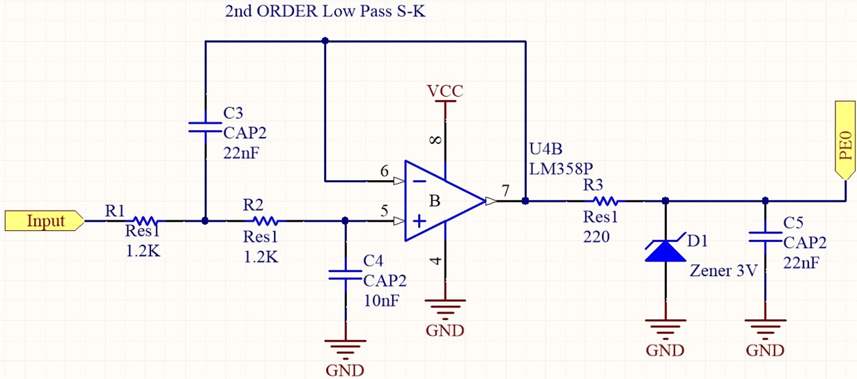
    One final doubt regarding the ADC's hardware.  I've added a 2nd order filter to my already-processed signal, with a cutoff frequency of approx 9kHz. (As I'm using a 2kHz sample rate in the ADC).

    Now, I've got some doubts regarding the use of the RC filter stage prior to the  ADC's input.

    If I'm not mistaken,  R3 and C5 (in my attached schematic) could be discarded, as it's redundant to re-filter what has already been filtered.  Is this correct? 

    Or am I missing some considerations regarding 'input impedance' issues, or something like that?

    (As far as I can tell, the "source impedance" seen by the ADC is the output impedance of the filter's Op Amp , i.e an extremely low one)

    Thanks again for taking the time to read this.

    Kind regards.

    Martín

  • Hello Martin,

    The maximum source impedance as seen by the ADC pin the TM4C123 is 500Ohms. So from an impedance perspective the above circuit is OK. Removing the RC is not going to affect the signal quality unless a fast transient is expected from sources adjacent to the output of the OPAMP

    Indeed cb1 and Robert's inputs are very important on this forum. They do bring a lot of practical expertise beyond vendor.

    Regards
    Amit
  • Martin Cunningham said:
    If I'm not mistaken,  R3 and C5 (in my attached schematic) could be discarded, as it's redundant to re-filter what has already been filtered.  Is this correct? 

    Maybe, it depends on the op-amps capability of driving a capacitive load.  The drive must be fast and stable, capable of completely charging or discharging the sample capacitor in the sample time (I'd have to check the data sheet, it's probably on the order of 0.1 uS).  The capacitor C5 does this by effectively providing close to zero impedance to the sample cap/sample resistor combo and providing enough capacitance that the charge required to change the sample capacitor voltage does not change the voltage on C5 significantly.  The resistor R3 essentially decouple the op-amp from the capacitor, usually improving stability. Both R3 and C5 are cheap, I'd leave them in the design, you can always depopulate C5 and replace R3 with a zero ohm resistor.  Patching them in if you've left them out of the design is a lot more difficult.

    R3/C5 also act as a single order low pass.  Potentially useful.

    Finally you need to retain R3 in order for D1 to be useful.

    Martin Cunningham said:
     I've added a 2nd order filter to my already-processed signal, with a cutoff frequency of approx 9kHz. (As I'm using a 2kHz sample rate in the ADC).

    This filter should be much slower.  Less than 1kHz to meet Nyquist although you can fool around with it a bit in practice.  In general though 1kHz or slower is needed to ensure that the signal you read matches the input to reasonable fidelity.

    Robert

  • It would appear - at the frequencies thus far mentioned - that a reasonable quality audio/signal generator may prove instructive in your testing.

    Also there are inexpensive ICs which are quite capable of serving well as a very low cost - yet quite capable test/signal generator - suited to your (assumed) sub 20KHz purposes.

    This vendor (and few others) have free or low cost, "SPICE" programs - which may greatly assist your circuit designs - especially component value confirmation.

    Thanks to Amit for his kind words - often the act of "explanation" strengthens understanding.

    What/When you "think" you understand - may very much differ from "real understanding" - especially when the car, MCU, or system misbehaves - and the real mystery reveals...