This thread has been locked.

If you have a related question, please click the "Ask a related question" button in the top right corner. The newly created question will be automatically linked to this question.

I2C connection with PCF8574 (Remote 8-Bit I/O Expander) to drive LED

Other Parts Discussed in Thread: PCF8574

Hello,

I am using TIVA C launch pad for my experiment. With reference to TIVA ware I2C example (loopback) mode I am configuring my application. Below is my schematic for the application.

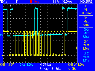
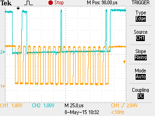
SCL and SDA line continuously stay low. Please let me is there any corrections I need to do in hardware.

Below is my code. Reference is taken from Tiwaware example , I'm kind of  stuck in it.

#include <stdbool.h>
#include <stdint.h>
#include "inc/hw_i2c.h"
#include "inc/hw_memmap.h"
#include "inc/hw_types.h"
#include "driverlib/gpio.h"
#include "driverlib/i2c.h"
#include "driverlib/pin_map.h"
#include "driverlib/sysctl.h"
#include "driverlib/uart.h"
#include "utils/uartstdio.h"

//*****************************************************************************
//
//! \addtogroup i2c_examples_list
//! <h1>I2C Master Loopback (i2c_master_slave_loopback)</h1>
//!
//! This example shows how to configure the I2C0 module for loopback mode.
//! This includes setting up the master and slave module.  Loopback mode
//! internally connects the master and slave data and clock lines together.
//! The address of the slave module is set in order to read data from the
//! master.  Then the data is checked to make sure the received data matches
//! the data that was transmitted.  This example uses a polling method for
//! sending and receiving data.
//!
//! This example uses the following peripherals and I/O signals.  You must
//! review these and change as needed for your own board:
//! - I2C0 peripheral
//! - GPIO Port B peripheral (for I2C0 pins)
//! - I2C0SCL - PB2
//! - I2C0SDA - PB3
//
// Number of I2C data packets to send.
//
//*****************************************************************************
#define NUM_I2C_DATA 3

//*****************************************************************************
//
// Set the address for slave module. This is a 7-bit address sent in the
// following format:
//                      [A6:A5:A4:A3:A2:A1:A0:RS]
//
// A zero in the "RS" position of the first byte means that the master
// transmits (sends) data to the selected slave, and a one in this position
// means that the master receives data from the slave.
//
//*****************************************************************************
#define SLAVE_ADDRESS 0x40

int
main(void)
{
    //
    // Set the clocking to run directly from the external crystal/oscillator.
    // TODO: The SYSCTL_XTAL_ value must be changed to match the value of the
    // crystal on your board.
    //
    SysCtlClockSet(SYSCTL_SYSDIV_1 | SYSCTL_USE_OSC | SYSCTL_OSC_MAIN |
                   SYSCTL_XTAL_16MHZ);

    //
    // The I2C0 peripheral must be enabled before use.
    //
    SysCtlPeripheralEnable(SYSCTL_PERIPH_I2C0);

    //
    // For this example I2C0 is used with PortB[3:2].  The actual port and
    // pins used may be different on your part, consult the data sheet for
    // more information.  GPIO port B needs to be enabled so these pins can
    // be used.
    // TODO: change this to whichever GPIO port you are using.
    //
    SysCtlPeripheralEnable(SYSCTL_PERIPH_GPIOB);

    //
    // Configure the pin muxing for I2C0 functions on port B2 and B3.
    // This step is not necessary if your part does not support pin muxing.
    // TODO: change this to select the port/pin you are using.
    //
    GPIOPinConfigure(GPIO_PB2_I2C0SCL);
    GPIOPinConfigure(GPIO_PB3_I2C0SDA);

    //
    // Select the I2C function for these pins.  This function will also
    // configure the GPIO pins pins for I2C operation, setting them to
    // open-drain operation with weak pull-ups.  Consult the data sheet
    // to see which functions are allocated per pin.
    // TODO: change this to select the port/pin you are using.
    //
    GPIOPinTypeI2CSCL(GPIO_PORTB_BASE, GPIO_PIN_2);
    GPIOPinTypeI2C(GPIO_PORTB_BASE, GPIO_PIN_3);

    //
    // Enable loopback mode.  Loopback mode is a built in feature that is
    // useful for debugging I2C operations.  It internally connects the I2C
    // master and slave terminals, which effectively let's you send data as
    // a master and receive data as a slave.
    // NOTE: For external I2C operation you will need to use external pullups
    // that are stronger than the internal pullups.  Refer to the datasheet for
    // more information.
    //
    HWREG(I2C0_BASE + I2C_O_MCR) |= 0x00;

    //
    // Enable and initialize the I2C0 master module.  Use the system clock for
    // the I2C0 module.  The last parameter sets the I2C data transfer rate.
    // If false the data rate is set to 100kbps and if true the data rate will
    // be set to 400kbps.  For this example we will use a data rate of 100kbps.
    //
    I2CMasterInitExpClk(I2C0_BASE, SysCtlClockGet(), false);

    // Tell the master module what address it will place on the bus when
    // communicating with the slave.  Set the address to SLAVE_ADDRESS
    // (as set in the slave module).  The receive parameter is set to false
    // which indicates the I2C Master is initiating a writes to the slave.  If
    // true, that would indicate that the I2C Master is initiating reads from
    // the slave.
    //
    I2CMasterSlaveAddrSet(I2C0_BASE, SLAVE_ADDRESS, false);


        // Place the data to be sent in the data register
        //
        I2CMasterDataPut(I2C0_BASE,0x00);

        //
        // Initiate send of data from the master.  Since the loopback
        // mode is enabled, the master and slave units are connected
        // allowing us to receive the same data that we sent out.
        //
        I2CMasterControl(I2C0_BASE, I2C_MASTER_CMD_SINGLE_SEND);

        // Wait until master module is done transferring.
        //
        while(I2CMasterBusy(I2C0_BASE))
        {
        }

        while(1)
        {

        }
}

  • May I commend you for that terrific drawing and a generally well written post?

    Confess that I've not time to (really) probe your code - yet concern rises due to your use of, "Loopback!"    Loopback normally is employed when external hardware is not (yet) ready/available.     That (apears) "not" your case - thus loopback may not be fully appropriate.     (our small firm never employs loopback - instead we insure that target hardware (or close substitute) always is present!)     (i.e. "nothing beats the real-world!)

    Suggest that you review the more normal/customary I2C API examples - not devoted to loopback - and repeat your test.    We've used a similar GPIO extender with excellent results.    Again congratulations on a well thought, caring post...

  • Hello Anup,

    I would suggest replacing the line

    HWREG(I2C0_BASE + I2C_O_MCR) |= 0x00;

    with

    HWREG(I2C0_BASE + I2C_O_MCR) = I2C_MCR_MFE;

    to make sure there is no residual code from previous run.

    Alternatively add the line

    SysCtlPeripheralReset(SYSCTL_PERIPH_I2C0);

    before

    SysCtlPeripheralEnable(SYSCTL_PERIPH_I2C0);

    and remove the MCR condition altogether.

    Regards
    Amit
  • Hello,

    Thank you for your suggestions.

    I did the suggested modifications and few more after seeing some examples.

    1) I have changed the pull up registers from 10kOhm to 4.7kOhm, because Vcc is 3.3 V (taken from TIVA C) so with 10kOhm voltage at SCL and SDA pin comes 1.8V and min voltage specified by the PCF8574 is 2.5V.

    2) Commented the HWREG statement.

    Below is the wave form I am getting.

    As per the main circuit schematic I need to put 0(zero) to make the LED glow. But Pin P0 on PCF8574 never goes down.

    I have tried it with burst command also but result remains the same. Please let me know if I am missing something.


    Below is my code;

    #include <stdbool.h>
    #include <stdint.h>
    #include "inc/hw_i2c.h"
    #include "inc/hw_gpio.h"
    #include "inc/hw_memmap.h"
    #include "inc/hw_types.h"
    #include "driverlib/gpio.h"
    #include "driverlib/i2c.h"
    #include "driverlib/pin_map.h"
    #include "driverlib/sysctl.h"
    #include "driverlib/uart.h"
    #include "utils/uartstdio.h"
    
    //! This example uses the following peripherals and I/O signals.  You must
    //! review these and change as needed for your own board:
    //! - I2C0 peripheral
    //! - GPIO Port B peripheral (for I2C0 pins)
    //! - I2C0SCL - PB2
    //! - I2C0SDA - PB3
    //
    // Number of I2C data packets to send.
    //
    //*****************************************************************************
    #define NUM_I2C_DATA 3
    
    //*****************************************************************************
    //
    // Set the address for slave module. This is a 7-bit address sent in the
    // following format:
    //                      [A6:A5:A4:A3:A2:A1:A0:RS]
    //
    // A zero in the "RS" position of the first byte means that the master
    // transmits (sends) data to the selected slave, and a one in this position
    // means that the master receives data from the slave.
    //
    //*****************************************************************************
    #define SLAVE_ADDRESS 0x40
    
    int
    main(void)
    {
        //
        // Set the clocking to run directly from the external crystal/oscillator.
        // TODO: The SYSCTL_XTAL_ value must be changed to match the value of the
        // crystal on your board.
        //
        SysCtlClockSet(SYSCTL_SYSDIV_1 | SYSCTL_USE_OSC | SYSCTL_OSC_MAIN |
                       SYSCTL_XTAL_16MHZ);
    
        //
        // The I2C0 peripheral must be enabled before use.
        //
        SysCtlPeripheralReset(SYSCTL_PERIPH_I2C0);
        SysCtlPeripheralEnable(SYSCTL_PERIPH_I2C0);
    
        //
        // For this example I2C0 is used with PortB[3:2].  The actual port and
        // pins used may be different on your part, consult the data sheet for
        // more information.  GPIO port B needs to be enabled so these pins can
        // be used.
        // TODO: change this to whichever GPIO port you are using.
        //
        SysCtlPeripheralEnable(SYSCTL_PERIPH_GPIOB);
    
        //
        // Configure the pin muxing for I2C0 functions on port B2 and B3.
        // This step is not necessary if your part does not support pin muxing.
        // TODO: change this to select the port/pin you are using.
        //
        GPIOPinConfigure(GPIO_PB2_I2C0SCL);
        GPIOPinConfigure(GPIO_PB3_I2C0SDA);
    
        //
        // Select the I2C function for these pins.  This function will also
        // configure the GPIO pins pins for I2C operation, setting them to
        // open-drain operation with weak pull-ups.  Consult the data sheet
        // to see which functions are allocated per pin.
        // TODO: change this to select the port/pin you are using.
        //
        GPIOPinTypeI2CSCL(GPIO_PORTB_BASE, GPIO_PIN_2);
        GPIOPinTypeI2C(GPIO_PORTB_BASE, GPIO_PIN_3);
    
        //
        // Enable loopback mode.  Loopback mode is a built in feature that is
        // useful for debugging I2C operations.  It internally connects the I2C
        // master and slave terminals, which effectively let's you send data as
        // a master and receive data as a slave.
        // NOTE: For external I2C operation you will need to use external pullups
        // that are stronger than the internal pullups.  Refer to the datasheet for
        // more information.
        //
     //   HWREG(I2C0_BASE + I2C_O_MCR) = I2C_MCR_MFE ;
    
        //
        // Enable and initialize the I2C0 master module.  Use the system clock for
        // the I2C0 module.  The last parameter sets the I2C data transfer rate.
        // If false the data rate is set to 100kbps and if true the data rate will
        // be set to 400kbps.  For this example we will use a data rate of 100kbps.
        //
        I2CMasterInitExpClk(I2C0_BASE, SysCtlClockGet(), false);
    
        // Tell the master module what address it will place on the bus when
        // communicating with the slave.  Set the address to SLAVE_ADDRESS
        // (as set in the slave module).  The receive parameter is set to false
        // which indicates the I2C Master is initiating a writes to the slave.  If
        // true, that would indicate that the I2C Master is initiating reads from
        // the slave.
        //
        I2CMasterSlaveAddrSet(I2C0_BASE, SLAVE_ADDRESS, false);
    
    
            // Place the data to be sent in the data register
            //
            I2CMasterDataPut(I2C0_BASE,0x01);
    
            //
            // Initiate send of data from the master.  Since the loopback
            // mode is enabled, the master and slave units are connected
            // allowing us to receive the same data that we sent out.
            //
         //   I2CMasterControl(I2C0_BASE, I2C_MASTER_CMD_BURST_SEND_START);
            //anup
            I2CMasterControl(I2C0_BASE, I2C_MASTER_CMD_SINGLE_SEND);
    
            // Wait until master module is done transferring.
            //
            while(I2CMasterBusy(I2C0_BASE)!=false)
           {
            	;
           }
    
            I2CMasterDataPut(I2C0_BASE,0x00);
    
                   //
                   // Initiate send of data from the master.  Since the loopback
                   // mode is enabled, the master and slave units are connected
                   // allowing us to receive the same data that we sent out.
                   //
                 I2CMasterControl(I2C0_BASE, I2C_MASTER_CMD_SINGLE_SEND);
                   //anup
                  // I2CMasterControl(I2C0_BASE, I2C_MASTER_CMD_SINGLE_SEND);
    
                   // Wait until master module is done transferring.
                   //
                   while(I2CMasterBusy(I2C0_BASE)!=false)
                  {
                   	;
                  }
    
    
            /*
    if(I2CMasterErr(I2C0_BASE)==I2C_MASTER_ERR_NONE)
    {
    	I2CMasterDataPut(I2C0_BASE,0x00);
    	I2CMasterControl(I2C0_BASE, I2C_MASTER_CMD_BURST_SEND_CONT);
    	 while(I2CMasterBusy(I2C0_BASE)!=false)
    	       {
    	        	;
    	       }
    	 I2CMasterDataPut(I2C0_BASE,0x00);
    	 I2CMasterControl(I2C0_BASE, I2C_MASTER_CMD_BURST_SEND_FINISH);
    }
    else
    {
    	I2CMasterControl(I2C0_BASE, I2C_MASTER_CMD_BURST_SEND_ERROR_STOP);
    }
    */
    }
    

  • anupsingh chandel said:
     have changed the pull up registers from 10kOhm to 4.7kOhm, because Vcc is 3.3 V (taken from TIVA C) so with 10kOhm voltage at SCL and SDA pin comes 1.8V and min voltage specified by the PCF8574 is 2.5V.

    May I observe that (something) is rotten with the result I've highlighted, above.      Is something else (unexpected) upon your I2C bus?     That great a change in voltage is abnormal - I'm wondering if your "read" of 10K was incorrect.     (100K, mistakenly installed - may explain)

    Have you (recently) measured the operating voltage @ your remote device's power pin?      And is ground properly routed between your MCU board - and your remote slave?

    Will leave that delightful "gob of code" to more motivated others.      Again "loopback" seems both unnecessary and a potential hindrance to your "live remote device" application - glad that you've eliminated it.     (you may check to insure that's (really) the case...)

  • Hello Anupsingh,

    Please check the slave address you are using. If you see in the waveform (Scope snpshot) the address is being NAK-ed.

    Regards
    Amit
  • Hi Amit,

    Might you (briefly) comment upon the (abnormal) drop reported while 10K pull-ups were employed?     We've used 10K for years - especially when battery powered - and consumption is an issue.    Iirc - Philips (I2C originator) spec does include 10K - does it not?
     
    Even a (horrible) slave address is unlikely to account for so drastic a voltage drop....

  • Frequency looks a little high, isn't the I/O expander an older chip, restricted to < 100kHz? Probably not a real issue though.

    I am kind of curious as to why you would choose an IIC I/O expander rather than a simple shift register. Are you running out of pins?

    A shift register is faster, simpler to use and less expensive.

    Robert
  • Hello cb1,

    I am not very clear with it so was waiting for an answer to your question first. With a 10K resistor the voltage should have dropped all the way to 0 and come up to 3.3V. With a stronger resistor it is the low level voltage that would be affected.

    Regards
    Amit
  • Robert Adsett said:
    A shift register is faster, simpler to use and less expensive.

    Aha - what you say is true - yet most (simple) shift registers "bounce/chain" their data - from output to output - which may cause unwanted results.    

    Superior types avoid that gremlin - at the cost of increased (and required) GPIO pin drive commitment.       (I'm thinking of HC595 as (proper) shifter - due to inclusion of storage register - which can prevent that signal "shift/bounce" from causing (unwanted) results.      Far older - HC164 "enjoyed" that bounce - due to the absence of storage register...     Glitched outputs - anyone?      Such may (almost) justify use of I2C (or SPI) style/type extenders....

  • The '595 is what I was thinking of, it never occurred to me to use an non-registered shift register. And although it does have extra pin inputs, there is no necessity to hook them up to the micro, they can be tied to the appropriate rails.

    A three wire connection to a '595 is quite easy. *Reset to power through a pull-up, *OE to ground. That leaves clock, data and chip select, the standard SPI complement.

    IIC does have a pin count advantage, but you can get essentially unlimited SPI connections with 5 pins, 3 pins if you simply want outputs using a '595.

    Robert
  • Robert Adsett said:
    That leaves clock, data and chip select, the standard SPI complement.

    It's been years since we used - but does that "3 wire" implementation to 595 escape (dreaded) "glitched while shifting" outputs?

    In fact - my small firm - on multiple occasions - chose the I2C expander route to insure that sufficient GPIO remained after (any) SIPO chip attachment.

  • cb1- said:
    It's been years since we used - but does that "3 wire" implementation to 595 escape (dreaded) "glitched while shifting" outputs?


    Yes. The documentation is a little less than straightforward but by using latch clock as the chip select the data will be moved from the internal register to the output register on the rising edge of the chip select (IE when de-selecting the chip).

    And of course they daisy chain nicely to get large numbers of output. Although practically speaking I don't think I've ever gone beyond 3 or 4 ICs.

    Robert
  • Amit Ashara said:
    the address is being NAK-ed

    This might be nitpicking, but I have a problem with the word selection here. If I'm not totally wrong, a NAK in I2C is a passive event, whereas an ACK is an active event. Thus, an ACKed address is a sign that the slave hears you and agrees on the address and is ready to serve. A NAK (rather a missing ACK) tells that either the slave doesn't hear you or the slave disagrees on the address or the slave is not ready to serve

    It's a small thing, but it's important to understand the difference especially when scratching your head on why things don't work.

    Not that I doubt you wouldn't know the difference Amit, but for the sake of any bystanders "on the learning curve" I thought I'd bring this up.

  • Hello Veikko

    "Familiarity breeds Contempt". I will take care of such information in my future posts. Thank you for correcting me.

    Regards
    Amit
  • Let this reporter register as, "equally familiar - and contemptible."

    Veikko - your word picture is extremely disciplined & precise. Clearly took time/effort to compose - really does enforce a "higher understanding" of what's (really) occurring.     I've "appropriated" for our firm's use - will hoist a tall one in your honor - merci...

  • De rien, mes amis.
  • And that (much hated) High School French teacher declared cb1's work, "uninspired!" Sacre bleu...
  • Hello,

    Thank you for your suggestions. I have verified it and it was 10k only.

    As per your suggestions I have ohm out the connections and it was okay.

    In below post I have seen that the wave forms are coming with 1.8V only and the user has kept 10k only.

    https://e2e.ti.com/support/microcontrollers/tiva_arm/f/908/t/364191

  • Hello Amit,

    Thank you for your suggestions. Yes I was making a mistake. The address should be 0x20 not 0x40 (which I was writing).

    The code is working now.

    But I am still confuse how to interpret 7 bit hexadecimal value. After referring some literature I got this 0x20 .

    Below is the wave form coming now.


  • Hello Anupsingh,

    The address is represented in 5 downto 0 format. But when packing it up for a byte it must be 8 bits. Secondly some data sheets show the R/W bit also as part of the address, Hence what is seen as 0x40 is actually 0x20.

    Regards
    Amit

  • Might (above poster) "Amot" have a (not so evil) twin?