This thread has been locked.
If you have a related question, please click the "Ask a related question" button in the top right corner. The newly created question will be automatically linked to this question.
DEAR ALL
i have two boards . one is Tm4c129x Dev Board another is our ev board with TM4C1294NCPDT cpu .
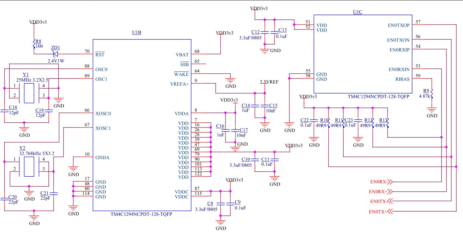
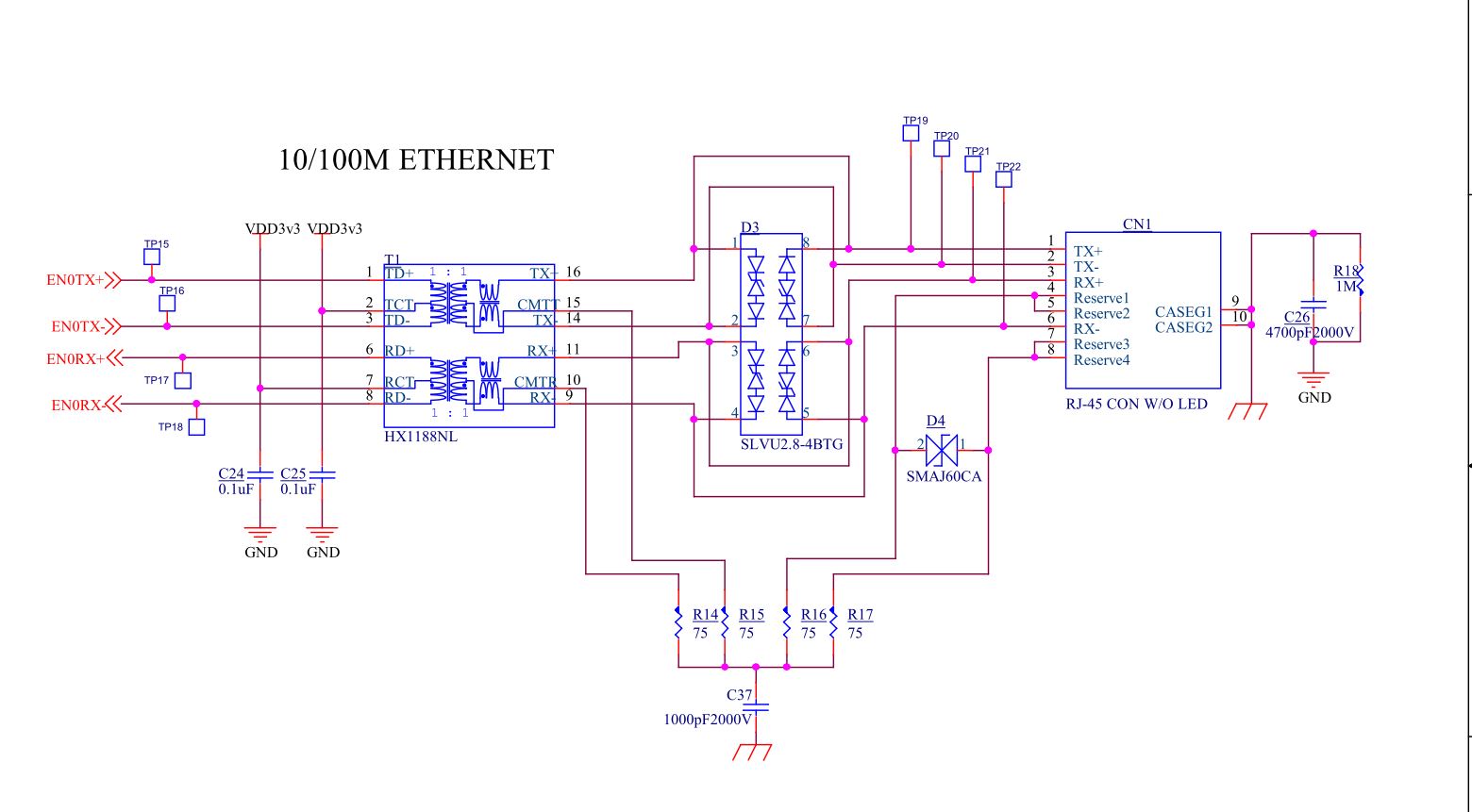
i run Ethernet well on Tm4c129x Dev Board . But Ethernet doesnt work on our ev-board with the same firmware .
The first thing i want to check is where is the problem ,firmware or hardware,?
Could i verify the Ethernet by bootloader in ROM instead of my own firmware?
If not , Could you give me some idea to check where is the issue .
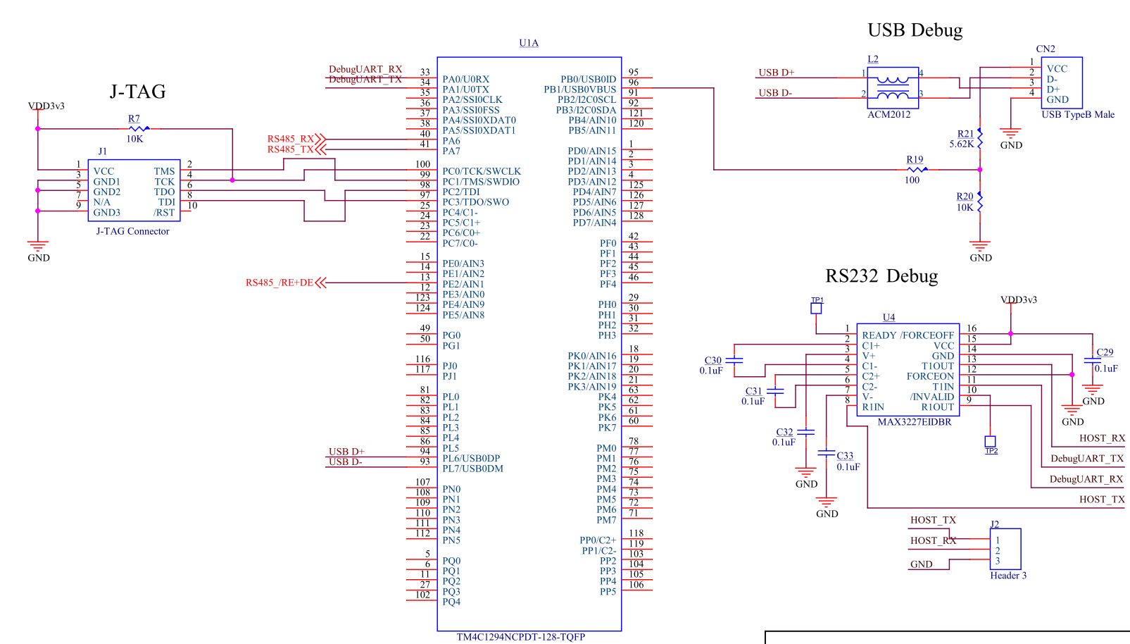
The second problem is about Jtag. i use the Tm4c129x Dev Board for ICDI debug shunt to my own ev-board. In the beginning i can burn the firmware well.
i don't change the hardware pin , but Lmflash show cant initial device forever . I found the TMS without pull high Resistance . Does it matter?
best regards
alex wang
Hi Alex,
Thanks for post schematic worth 1000's words alone.
Couple questions;
Why no Vbat series resistor (51ohm) and (.1uf) to GND mounted near pin 68, insures very critical voltage rise time requirement into MPU?
Reset pin with zener diode alone may not give ample reset period, Typical is GND__/ --100ohm--10k^(VDD)--Pin70--.1uf GND. (DS page 1834)
Does your Dev board have Y2 same 32Mhz?
Check external Vref (DS page 1858); vRef @+2.4v is minimum and requires CTL register settings.
Hope these checks help.
Later notice missing 2k series resistor into OSC1 pin 89, Do insure 25Mhz oscillates at the correct frequency.
May we note that your post would have (also) benefitted from the same (schematic) form urged upon poster?
Shorthand/symbol form you employ may not prove universal. To illustrate - what does your, "GND__/ --100ohm--10k^(VDD" really convey? It seems to suggest that 100Ω ties to 10K - w/that resistive pair bounded by ground & Vdd (yielding a very small voltage) - was that your intent?
This may better convey your meaning: (that's a momentary switch w/redundant contacts - used in multiple of our firm's products)
Believe you can get a schematic editor (free) bundled w/in a, "Design Simulator" package from this vendor or (similar) others.
As poster complains of, "NO JTAG" - and has not installed external (far lower resistance) pull-up Rs - he bears some responsibility. Quick/free ain't (always) best!
Take it PB1 is the input leading to MPU reset pin 70.
Should Alex not be programming the hibernate module Y2 might can be removed and ground pin 66 OSC0, WAKE pin 64 is already at ground. Wake being grounded with Y2 installed seems oddly out of place since PIOS can provide 16Mhz for both ADC clock and WDT1.
Pin 64 often has pull up of 1 megohm connected to VDD when Y2 is added. That makes ready the hibernate module to program. Unless your program configures the real time clock or hibernate module why is Y2 even needed?
Removing Y2 eliminates the requirement to delay +Vbat and removes need to add .1uf capacitor, 51 ohm series resistor.
Read today the ROM boot loader my enable USB pins 93/94 (page 1822) when flash is erased. Suspect to start a binary file transfer in response to a ping request. Think that ping control is similar to a magic packet sent by the server during Bootp hand shake.