This thread has been locked.

If you have a related question, please click the "Ask a related question" button in the top right corner. The newly created question will be automatically linked to this question.

Tiva 4C129 BOOTCFG issues

Other Parts Discussed in Thread: TM4C1294NCPDT, LMFLASHPROGRAMMER, UNIFLASH, EK-TM4C1294XL, TM4C129XNCZAD

Greetings,

I have searched the forums and found similar posts but none of them addressed my issue so I'm posting yet another one here.

Using Tiva C TM4C1294NCPDT on Launchpad TM4C1294XL, am  unable to repeatedly program BOOTCFG register or trigger a boot using a pin.   I managed to program the bootcfg once, but am not sure how because I cannot reprogram it.

Goal is to drive GPIO PB4 low as boot trigger, reset and then bootload on the Uart 0 port.

* Using default key 0xA442 per the data sheet for BOOTCFG.

* Want to bootload using PB4 grounded when reset occurs.
* Setting all reserved bits high in register writes.
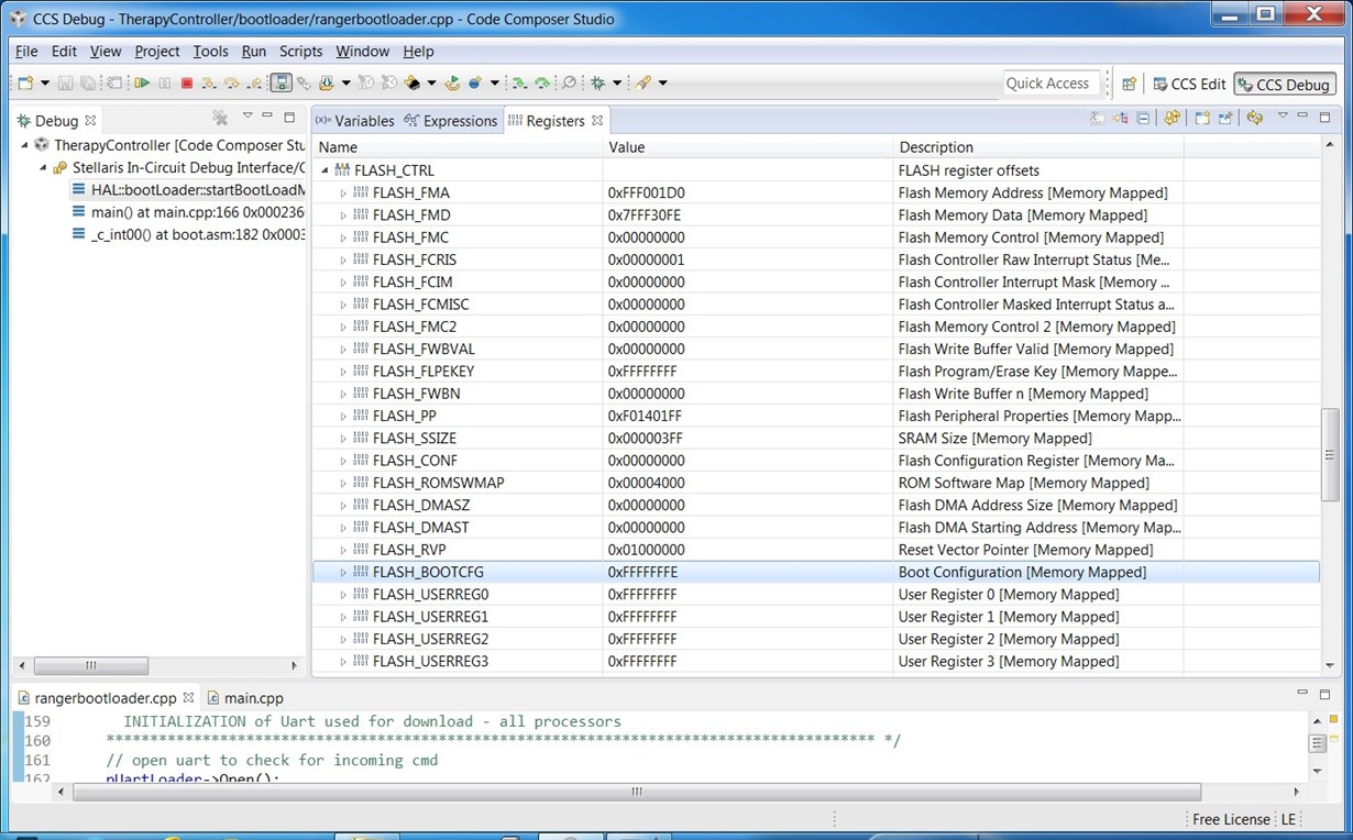
* BOOTCFG currently reported by ccs to be 0x7FFF30FE but can't be changed!

Using code composer studio and can therefore view the contents of the flash registers while stepping thru the code.

* Per data sheet, FLASHCTRL_BASE = 0x400FD000
FMA_OFFSET = 0x000
FMD_OFFSET = 0x004
FMC_OFFSET = 0x008
BOOTCFG_OFFSET = 0x01D0

=================================================================
SEQUENCE - please verify this is correct for writing to BOOTCFG
=================================================================

// ===================================================
// 1. Write BOOTCFG offset to FMA register 0x400FD000
// FMA: D31-D20 RESERVED, D19-D0 OFFSET
// ===================================================
*((volatile uint32_t *)(0x400FD000)) = (uint32_t)0xFFF001D0;   // this 

// =================================================
// 2 . Write bootcfg data to FMD register 0x400FD004.
// D31-D0 DATA
// =================================================
//*((volatile uint32_t *)(0x400FD004)) = (uint32_t)0x7FFF30FE;
*((volatile uint32_t *)(0x400FD004)) = (uint32_t)0x7FFFFFFE;

//=======================================================================
// 3. Write FMC register 0x400FD008
// D31-D16 WRKEY, D15-D4 reserved, D3 COMT, D2 MERASE, D1 ERASE, D0 WRITE
//=======================================================================
*((volatile uint32_t *)(0x400FD008)) = (uint32_t)0xA442FFF0; // tried setting write and commit here also
*((volatile uint32_t *)(0x400FD008)) |= (uint32_t)0x1; // set WRITE
*((volatile uint32_t *)(0x400FD008)) |= (uint32_t)0x8; // set COMMIT


========
details
========

Using CCS, registers FMA and FMD can be seen to change when written to.

FMC never changes and stays all zeros in the ccs register window.
when FMC is written to, register FLASH_FCRIS is seen to change to a value of 3

Currently BOOTCFG is set to 0x7FFF30FE which means a low on PB4 during reset
should force the ROM bootloader to execute. It does not do so but my code which
flashes LEDs does not run either. Seems to go into the weeds. The bootloader
download command sent from a windows side program to Tiva Uart 0 receives no reply.
If I call the ROM bootload function in my code on the target, the windows side download command
works fine (using Uart 0 on Tiva) and reflash works.

When I attempt the pin triggered bootload, I ground PB4 then power up the launchpad
then push launchpad reset button then start the windows application.

What am I doing incorrectly?

Thanks

Randall Miner (randall_miner@jabil.com)

  • Hello Randy,

    U20 PA0 (RX) connects to VCP_RXD, which via R6 connects to TARGET_TXD which connects to PA1 (TX) of TM4C129.

    Also by removing the jumpers as well you can get to the same function.

    Regards
    Amit
  • Hi Amit,

    I got all this working by following your suggestion of removing the two jumpers to Uart 0 and by enabling the autobaud.
    There is one last question I have concerning the NW bit in the BOOTCFG register. I know you said this thread is getting too long. How can I contact you directly? I accepted the friend request.
  • Hello Randall

    Since it may be a generic discussion, you may post it on the forum. However if it is very specific to your application and discussion involves discussing NDA content then we can move it to conversations on the top-right corner of the forum web page.

    Regards
    Amit
  • Amit,

    Two questions.

    First, I am not clear on what bit 31 NW of the BOOTCFG is telling us.  Datasheet shows it as a RO (read only).

    "The NW bit indicates that bits in the register can be changed from 1 to 0."

    When are the BOOTCFG bits not modifiable even though they are all ones.   I was able to modify my bootcfg on two of my boards but for the other two I cannot.

    BOOTCFG is stuck at all FFs.  Yes I know a power cycle is required before changes can be seen.

    Here is the screenshot and below it, the code.  I have writing 0xFFFF30FE and 0x7FFF30FE to bootcfg.  Neither results in a change.  Not sure how I got this to work on the first two boards.

    Page 614 in the data sheet says:

    The register contents are unaffected by any reset condition except power-on reset, which returns the register contents to 0xFFFF.FFFE
    for the BOOT Configuration (BOOTCFG) register and 0xFFFF.FFFF for all others.

    By committing the register values using the COMT bit in the Flash Memory Control (FMC) register,
    the register contents become non-volatile and are therefore retained following power cycling. Once
    the register contents are committed, the only way to restore the factory default values is to perform
    the sequence described in “Recovering a "Locked" Microcontroller” on page 213.

    ======================

    The NW bit indicates that bits in the register can be changed from 1 to 0.

    ======================

    Bit/Field Name Type Reset Description
    31 NW RO 1 Not Written
    When set, this bit indicates that the values in this register can be changed
    from 1 to 0. When clear, this bit specifies that the contents of this register
    cannot be changed


    #define FLASH_BOOTCFG_FACTORY_DEFAULT 0xFFFFFFFE

    // selecting GPIO PB4 active low for trigger of bootloader following hardware reset
    #define FLASH_BOOTCFG_VALUE_R 0xFFFF30FE
    #define FMA_BOOTCFG_ADDR 0xFFF001D0 // offset of BOOTCFG 0x01D0 with reserved bits of register set high. 0xFFF01D0
    #define FMC_WRITEVALUE_R 0xA442FFF0 // FMC_DEFAULT_KEY | FMC_RESERVED_BITS

    //#define SYSCNTL_BASE_ADDR 0x400FE000
    #define FLASHCTRL_BASE 0x400FD000 // FLASH Controller

    #define FMA_OFFSET 0x000
    #define FMD_OFFSET 0x004
    #define FMC_OFFSET 0x008
    #define FLPEKEY_OFFSET 0x03C
    #define BOOTCFG_OFFSET 0x01D0
    #define FMA_RESERVED_BITS 0xFFF00000

    #define FMA_ADDR (FLASHCTRL_BASE + FMA_OFFSET)
    #define FMD_ADDR (FLASHCTRL_BASE + FMD_OFFSET)
    #define FMC_ADDR (FLASHCTRL_BASE + FMC_OFFSET)
    #define FLPEKEY_ADDR (FLASHCTRL_BASE + FLPEKEY_OFFSET)
    #define FLPEKEY_DATA 0xFFFFA442

    // **************************
    // FMC defines and macros
    // **************************
    #define FMC_WR (uint32_t)0x01
    #define FMC_COMT (uint32_t)(0x01 << 3)
    #define FMC_DEFAULT_KEY (uint32_t)(0xA442 << 16)
    #define FMC_RESERVED_BITS(uint32_t)(0xFFF << 4)

    // **************************************************************
    // these methods are for programming the BOOTCFG
    // **************************************************************
    void HAL::bootLoader::programBOOTCFG(bool enableBootPin)
    {
    uint32_t bootcfgNewVal = 0;

    if(enableBootPin)
    {

    bootcfgNewVal = static_cast<uint32_t>(FLASH_BOOTCFG_VALUE_R); // offset of BOOTCFG 0x01D0 with reserved bits of register set high. 0xFFF01D0
    }
    else
    {
    bootcfgNewVal = static_cast<uint32_t>(FLASH_BOOTCFG_FACTORY_DEFAULT);
    }

    // ===================================================
    // 1. Write BOOTCFG address to FMA register 0x400FD000
    // ===================================================
    wrRegFMA( FMA_BOOTCFG_ADDR );

    // =================================================
    // 2 . Write source data to FMD register 0x400FD004.
    // =================================================
    wrRegFMD( bootcfgNewVal );

    //================================
    // 3. Write FMC register 0x400FD008
    //================================
    wrRegFMC( FMC_WRITEVALUE_R );

    }

    // ===================================================
    // FMA register 0x400FD000
    // ===================================================
    // RRRR RRRR RRRR OOOO OOOO OOOO OOOO OOOO O = register offset of register we are programming.
    void HAL::bootLoader::wrRegFMA(uint32_t newvalue)
    {
    wrMem32(FMA_ADDR, newvalue);
    }

    // =================================================
    // FMD register 0x400FD004.
    // =================================================
    // data to be written to the flash register. write the value we want to go into the BOOTCFG here.
    // DDDD DDDD DDDD DDDD DDDD DDDD DDDD DDDD
    void HAL::bootLoader::wrRegFMD(uint32_t newvalue)
    {
    wrMem32(FMD_ADDR, newvalue);
    }

    //================================
    //FMC register 0x400FD008
    //================================
    // 1001 0100 0100 0010 1111 1111 1111 1001 0xA442FFF9
    // KKKK KKKK KKKK KKKK RRRR RRRR RRRR CMEW

    // K = WRKEY D31-D16 USE 0xA442 IF BOOTCFG KEY bit set to one (default key)
    // C = COMT D3
    // 0 = no effect. 1= Set this bit to commit (write) the register value to a Flash-memory-resident register.
    // When read, a 1 indicates that the previous commit access is not complete.
    // M = MERASE D2 Mass Erase Flash Memory 0 has no effect on the state of this bit. 1= erase the Flash main memory.
    // E = ERASE D1 Erase a Page of Flash Memory 0 has no effect 1 = Set this bit to erase the Flash memory page specified by the contents of the FMA register
    // W = WRITE D0 Write a Word into Flash Memory 0 has no effect 1 = Set this bit to write the data stored in the FMD register into the Flash memory location specified by the contents of the FMA register.
    void HAL::bootLoader::wrRegFMC(uint32_t newvalue)
    {
    wrMem32(FMC_ADDR, newvalue); // write the newvalue

    // data sheet documentation is not clear on whether or not WR and COMT need to be set in a particular order. Setting WR the COMT seems logical.
    wrMem32( FMC_ADDR, (rdMem32(FMC_ADDR) | FMC_WR) ); // set WR bit

    wrMem32( FMC_ADDR, (rdMem32(FMC_ADDR) | FMC_COMT ) ); // set COMT bit

    while( ( rdMem32(FMC_ADDR) & FLASH_FMC_COMT) == FLASH_FMC_COMT) { }

    }

    uint32_t HAL::bootLoader::rdMem32(uint32_t addr)
    {
    return ( *( (volatile uint32_t *)(addr) ) );
    }

    void HAL::bootLoader::wrMem32(uint32_t addr, uint32_t newvalue)
    {
    ( *( (volatile uint32_t *)(addr) ) ) = newvalue;
    }

  • Hello Randall

    Is this the function for the BOOTCFG commit operation? If yes, then I think it is wrong.

    void HAL::bootLoader::wrRegFMC(uint32_t newvalue)
    {
    wrMem32(FMC_ADDR, newvalue); // write the newvalue

    // data sheet documentation is not clear on whether or not WR and COMT need to be set in a particular order. Setting WR the COMT seems logical.
    wrMem32( FMC_ADDR, (rdMem32(FMC_ADDR) | FMC_WR) ); // set WR bit

    wrMem32( FMC_ADDR, (rdMem32(FMC_ADDR) | FMC_COMT ) ); // set COMT bit

    while( ( rdMem32(FMC_ADDR) & FLASH_FMC_COMT) == FLASH_FMC_COMT) { }

    }

    Regards
    Amit
  • yes that is it.   What needs corrected?

    Regards,
    Randy

  • Hello Randall,

    This is the code for Commit of the BOOTCFG

    HWREG(FLASH_FMA) = 0x75100000;
    HWREG(FLASH_FMD) = newvalue;
    HWREG(FLASH_FMC) = FLASH_FMC_WRKEY | FLASH_FMC_COMT;

    while(HWREG(FLASH_FMC) & FLASH_FMC_COMT)
    {
    }

    Regards
    Amit
  • I saw that on the forum and thought it applied to another processor, not Tiva.  The address makes no sense according to the data sheet.  Perhaps I changed it in my code and that's why I was able to program the bootcfg before.

    Where does this value  0x75100000 come from?

    HWREG(FLASH_FMA) = 0x75100000;

    BOOTCFG Offset = 0x1D0 from page 674 of data sheet TMC4C1294NCPDT.
    Inline image 2

    reserved are to be set to all ones per advice on the forum.

    Thus I used the value of 0xFFF001D0


    Inline image 1

    Regards,

    Randy


    ------------------------------------------------------------------------
     Randall D. Miner,   Embedded SW Engineer contractor.
     Randstad Technologies.
     2050 Spectrum Blvd.  Ft. Lauderdale  FL. 33309
     cell (954)-812-8180    ofc (954) 828-2770
     Reports To: Ron Reinhart(JABIL) & Steve Machan (RT)
    ------------------------------------------------------------------------

  • Hello Randall

    In the Internal memory Chapter please look for Table 8.3 "User-Programmable Flash Memory Resident Registers" and description of the commit operations in section 8.2.3.12 "Non-Volatile Register Programming-- Flash Memory Resident Registers". I am referring to the TM4C129XNCZAD data sheet but it should be the same for the device you have.

    As for the value 0x75100000, I have no clue as to why this was selected.

    Regards
    Amit
  • very confusing to have the upper bits marked as "reserved" when apparently they are only reserved for volatile registers.

    Regards,

    Randy


    ------------------------------------------------------------------------
     Randall D. Miner,   Embedded SW Engineer contractor.
     Randstad Technologies.
     2050 Spectrum Blvd.  Ft. Lauderdale  FL. 33309
     cell (954)-812-8180    ofc (954) 828-2770
     Reports To: Ron Reinhart(JABIL) & Steve Machan (RT)
    ------------------------------------------------------------------------

  • Hello Randall

    For most functional operations like Program and Erase, the FMA is limited to the address space of the TM4C129x device. The Commit Operations are special operations and handled by the FMC Commit Bit. So in most respect it is OK to have the upper bits reserved.

    Regards
    Amit
  • understood thank you so much for all the help.

    Regards,
    Randy

  • Hello! Help me plz. This is my test code, but hi does not work correctly. After reset BOOTCFG is right, but in Keil i see "Fault ISR", what's wrong?


    int
    main(void)
    {
    uint32_t ui32SysClock;

    ui32SysClock = SysCtlClockFreqSet((SYSCTL_XTAL_25MHZ |
    SYSCTL_OSC_MAIN |
    SYSCTL_USE_PLL |
    SYSCTL_CFG_VCO_480), 120000000);


    PinoutSet();


    ROM_UARTConfigSetExpClk(UART0_BASE, ui32SysClock, 115200,
    (UART_CONFIG_PAR_NONE | UART_CONFIG_STOP_ONE |
    UART_CONFIG_WLEN_8));

    ROM_UARTEnable(UART0_BASE);


    HWREG(FLASH_FMA) = 0x75100000;
    HWREG(FLASH_FMD) = newvalue;
    HWREG(FLASH_FMC) = FLASH_FMC_WRKEY | FLASH_FMC_COMT;

    while(HWREG(FLASH_FMC) & FLASH_FMC_COMT)
    {}
    while(1)
    {
    //

    GPIOPinWrite(GPIO_PORTK_BASE, GPIO_PIN_2, GPIO_PIN_2);

    ROM_SysCtlDelay(10000000);


    GPIOPinWrite(GPIO_PORTK_BASE, GPIO_PIN_2, 0);

    ROM_SysCtlDelay(10000000);
    }

    return(0);
    }
  • Hi Alex,

    Nothing stands out as being wrong.

    When I"ve gotten the fault isr,  I've found the best approach is to use the code composer debugger to single step over each line of C code in your main.cpp until you find the last line before the fault occurs.  In that line of code, something is incorrect which is triggering a processor exception.

    Here is a link to a texas instruments document that might help you also...

    good luck!

    R. Miner

  • Hello Randall

    Rather obvious in the code. The SysCtlPeripheralEnable is not being called. So my bet would be at UART0 register programming to be generating the bus fault

    Regards
    Amit
  • Good day.

    I am add ROM_SysCtlPeripheralEnable(SYSCTL_PERIPH_UART0), but again I see "FaultISR".

    NVIC_FAULT_STAT - 0x00000400

    NVIC_BUS_FAULT_ADDR - 0xE000EDF8

    But this mean that error in "Cortex-M4F Peripherals (SysTick, NVIC,MPU, FPU and SCB)" . What to do next?

  • Sorry, I forgot to write int newvalue = FLASH_BOOTCFG_NW|FLASH_BOOTCFG_PORT_A|FLASH_BOOTCFG_PIN_2|FLASH_BOOTCFG_KEY|FLASH_BOOTCFG_DBG1|FLASH_BOOTCFG_EN;
  • Hello Alex,

    I am sorry but I did not understand what the newvalue has to got to do with the UART0. Can you attach the updated code?

    Regards
    Amit
  • This is my code :

    int newvalue = FLASH_BOOTCFG_NW|FLASH_BOOTCFG_PORT_A|FLASH_BOOTCFG_PIN_2|FLASH_BOOTCFG_KEY|FLASH_BOOTCFG_DBG1|FLASH_BOOTCFG_EN;//

    //*****************************************************************************
    //
    // The error routine that is called if the driver library encounters an error.
    //
    //*****************************************************************************
    //#ifdef DEBUG
    //void
    //__error__(char *pcFilename, unsigned long ulLine)
    //{
    //}
    //#endif

    //*****************************************************************************
    //
    // A simple application demonstrating use of the boot loader,
    //
    //*****************************************************************************
    int
    main(void)
    {
    uint32_t ui32SysClock;

    //
    // Run from the PLL at 120 MHz.
    //
    ui32SysClock = SysCtlClockFreqSet((SYSCTL_XTAL_25MHZ |
    SYSCTL_OSC_MAIN |
    SYSCTL_USE_PLL |
    SYSCTL_CFG_VCO_480), 120000000);

    //
    // Configure the device pins.
    //
    PinoutSet();

    //
    // Enable the UART that will be used for the firmware update.
    //
    ROM_SysCtlPeripheralEnable(SYSCTL_PERIPH_UART0);

    //
    // Configure the UART for 115200, 8-N-1.
    //
    ROM_UARTConfigSetExpClk(UART0_BASE, ui32SysClock, 115200,
    (UART_CONFIG_PAR_NONE | UART_CONFIG_STOP_ONE |
    UART_CONFIG_WLEN_8));

    //
    // Enable the UART operation.
    //
    ROM_UARTEnable(UART0_BASE);

    //


    // if (ROM_GPIOPinRead(GPIO_PORTA_BASE, GPIO_PIN_2 )==0)
    // {
    // HWREG(NVIC_DIS0) = 0xffffffff;
    // HWREG(NVIC_DIS1) = 0xffffffff;
    // HWREG(NVIC_DIS2) = 0xffffffff;
    // HWREG(NVIC_DIS3) = 0xffffffff;
    // HWREG(NVIC_DIS4) = 0xffffffff;

    // //
    // // Call the ROM UART boot loader.
    // //
    // ROM_UpdateUART();
    // }

    HWREG(FLASH_FMA) = 0x75100000;
    HWREG(FLASH_FMD) = newvalue;
    HWREG(FLASH_FMC) = FLASH_FMC_WRKEY | FLASH_FMC_COMT;

    while(HWREG(FLASH_FMC) & FLASH_FMC_COMT)
    {}
    while(1)
    {

    GPIOPinWrite(GPIO_PORTK_BASE, GPIO_PIN_2, GPIO_PIN_2);
    //
    // Delay for a while.
    //
    ROM_SysCtlDelay(10000000);

    //
    // Set the GPIO low.
    //

    GPIOPinWrite(GPIO_PORTK_BASE, GPIO_PIN_2, 0);
    //
    // Delay for a while.
    //
    ROM_SysCtlDelay(10000000);
    }
    //
    // The boot loader should not return. In the off chance that it does,
    // enter a dead loop.
    //
    return(0);
    }

    and my progectboot_demo_uart.rar

  • Hello Alex

    The BOOTCFG pin which is to be used for ROM call has to be asserted at Power On Reset or Pad Reset. Only then will the device continue to remain in ROM Boot Loader.

    Regards
    Amit
  • hello Amit.
    After loading my progect, I reboot my device. Then MCU wrine bootcfg to ROM. After reboot in degug I see "Fault ISR".
    Сan I not understand you?
  • Hello Alex,

    So is the Bus Fault coming when the device is in ROM Boot Loader before the new application is sent or it goes to Bus Fault after the new application is loaded?

    Regards
    Amit
  • Hello Amit
    After new application is loaded, and i may load new application only after reset bootcfg-register.
  • Hello Alex,

    Yes. You need to assert the Port and Pin to the correct BOOT polarity as configured in the BOOTCFG register, apply a reset, wait for few 10's of ms (At least) and then load the new application code.

    Regards
    Amit
  • Hello Amit.

    It did not help. After loading application does not work. For logick application, if PA2 = "0", we load new application, if PA=2= "1", we bling. But this  code after reboot give me only "Fault ISR" =(

  • Alex,

    I recommend you use a debugger to step thru your code one line at a time starting at the first line in main.cpp

    When you get to the line of code that is causing the fault and you step over that line,  the fault will occur.

    This will tell you the exact line of code causing the problem.  Then you can look at that line and hopefully see what is wrong.

    If you can't figure out why the line is causing a fault,  post the line of code that you know caused it, here.

    I know its possible find out the origin of the fault using this method because I've done it several times using code composer studio.

    R. Miner, Sr. Embedded Engineer & contractor.

  • R. Miner,
    The Fault ISR begin before first line.

    Without this code, application work:
    // HWREG(FLASH_FMA) = 0x75100000;
    // HWREG(FLASH_FMD) = newvalue;
    // HWREG(FLASH_FMC) = FLASH_FMC_WRKEY | FLASH_FMC_COMT;

    // while(HWREG(FLASH_FMC) & FLASH_FMC_COMT)
    // {}

    The code with this bootloader work :
    if (ROM_GPIOPinRead(GPIO_PORTA_BASE, GPIO_PIN_2 )==0)
    {
    HWREG(NVIC_DIS0) = 0xffffffff;
    HWREG(NVIC_DIS1) = 0xffffffff;
    HWREG(NVIC_DIS2) = 0xffffffff;
    HWREG(NVIC_DIS3) = 0xffffffff;
    HWREG(NVIC_DIS4) = 0xffffffff;

    //
    // Call the ROM UART boot loader.
    //
    ROM_UpdateUART();
    }
  • int main(void)
    {
       // my first line
    So you are saying it happens on entry to main?  But by commenting out lines below, the fault is fixed?

    Regards,
    Randy
     

  • Yea it happens befor enter to main. Yes, if i commenting this code :
    / HWREG(FLASH_FMA) = 0x75100000;
    // HWREG(FLASH_FMD) = newvalue;
    // HWREG(FLASH_FMC) = FLASH_FMC_WRKEY | FLASH_FMC_COMT;

    // while(HWREG(FLASH_FMC) & FLASH_FMC_COMT)
    // {}

    The application is work? and fault is fixed. Maybe in my TM4C1294 the ROM with bootloader is clear?
  • Hello Randall,

    That does not make sense. Writing to the BOOTCFG register should not create a Fault!

    Regards
    Amit
  • I think you misunderstood me.   I was simply telling him to use a debugger to step thru his code if he can't find the reason for his fault and I was asking him to clarify where he thinks the fault originates from.
    I will let you handle it.

    Regards,
    Randy
  • Hello Randy,

    That is what I am trying to ascertain from the poster as well.

    Regards
    Amit
  • Understood Amit.

    Alex,

    Here is code that works for my project. Amit helped me to get this working a few months ago. Hopefully I pasted all the defines in. Can't give you the complete file because it contains proprietary code.

    Hope it helps you.

    R. Miner

    #define FLASHCTRL_BASE 0x400FD000 // FLASH Controller

    #define FMA_OFFSET 0x000
    #define FMD_OFFSET 0x004
    #define FMC_OFFSET 0x008
    #define FLPEKEY_OFFSET 0x03C
    #define BOOTCFG_OFFSET 0x01D0
    #define FMA_RESERVED_BITS 0xFFF00000

    #define FMA_ADDR (FLASHCTRL_BASE + FMA_OFFSET)
    #define FMD_ADDR (FLASHCTRL_BASE + FMD_OFFSET)
    #define FMC_ADDR (FLASHCTRL_BASE + FMC_OFFSET)
    #define FLPEKEY_ADDR (FLASHCTRL_BASE + FLPEKEY_OFFSET)
    #define FLPEKEY_DATA 0xFFFFA442

    // **************************
    // FMC defines and macros
    // **************************
    #define FMC_WR (uint32_t)0x01
    #define FMC_COMT (uint32_t)(0x01 << 3)
    #define FMC_DEFAULT_KEY (uint32_t)(0xA442 << 16)
    #define FMC_RESERVED_BITS(uint32_t)(0xFFF << 4)


    // ********************************************************************************************************
    // these methods are for programming the BOOTCFG
    // must power cycle for these changes to take effect.
    // on the rising edge of reset, if the pin programmed into bootcfg is asserted, the ROM bootloader will run.
    // ********************************************************************************************************
    void HAL::bootLoader::programBOOTCFG(bool enableBootPin)
    {
    uint32_t bootcfgNewVal = 0;

    // program default key 0xA442 into FLPEKEY register offset 0x03C 0x400FD03C
    // *((volatile uint32_t *)(0x400FD03C)) = (uint32_t)0xFFFFA442;

    if(enableBootPin)
    {

    bootcfgNewVal = static_cast<uint32_t>(bootcfgValue); // offset of BOOTCFG 0x01D0 with reserved bits of register set high.
    }
    else
    {
    // this does not work and does nothing - it cannot be reset this way.
    bootcfgNewVal = static_cast<uint32_t>(FLASH_BOOTCFG_FACTORY_DEFAULT);
    }

    // ===================================================
    // 1. Write BOOTCFG address to FMA register 0x400FD000
    // ===================================================
    wrRegFMA( FMA_BOOTCFG_ADDR );

    // =================================================
    // 2 . Write bootcfg data to FMD register 0x400FD004.
    // =================================================
    wrRegFMD( bootcfgNewVal );

    //================================
    // 3. Write FMC register 0x400FD008
    //================================
    wrRegFMC( FLASH_FMC_WRKEY | FLASH_FMC_COMT );

    }

    // ===================================================
    // FMA register 0x400FD000
    // ===================================================
    // RRRR RRRR RRRR OOOO OOOO OOOO OOOO OOOO O = register offset of register we are programming.
    void HAL::bootLoader::wrRegFMA(uint32_t newvalue)
    {
    wrMem32(FMA_ADDR, newvalue);
    }

    // =================================================
    // FMD register 0x400FD004.
    // =================================================
    // data to be written to the flash register. write the value we want to go into the BOOTCFG here.
    // DDDD DDDD DDDD DDDD DDDD DDDD DDDD DDDD
    void HAL::bootLoader::wrRegFMD(uint32_t newvalue)
    {
    wrMem32(FMD_ADDR, newvalue);
    }

    //================================
    //FMC register 0x400FD008
    //================================
    // 1001 0100 0100 0010 1111 1111 1111 1001 0xA442FFF9
    // KKKK KKKK KKKK KKKK RRRR RRRR RRRR CMEW

    // K = WRKEY D31-D16 USE 0xA442 IF BOOTCFG KEY bit set to one (default key)
    // C = COMT D3
    // 0 = no effect. 1= Set this bit to commit (write) the register value to a Flash-memory-resident register.
    // When read, a 1 indicates that the previous commit access is not complete.
    // M = MERASE D2 Mass Erase Flash Memory 0 has no effect on the state of this bit. 1= erase the Flash main memory.
    // E = ERASE D1 Erase a Page of Flash Memory 0 has no effect 1 = Set this bit to erase the Flash memory page specified by the contents of the FMA register
    // W = WRITE D0 Write a Word into Flash Memory 0 has no effect 1 = Set this bit to write the data stored in the FMD register into the Flash memory location specified by the contents of the FMA register.
    void HAL::bootLoader::wrRegFMC(uint32_t newvalue)
    {
    wrMem32(FMC_ADDR, newvalue); // write the newvalue

    while( ( rdMem32(FMC_ADDR) & FLASH_FMC_COMT) == FLASH_FMC_COMT) { }

    }


    uint32_t HAL::bootLoader::rdMem32(uint32_t addr)
    {
    return ( *( (volatile uint32_t *)(addr) ) );
    }

    void HAL::bootLoader::wrMem32(uint32_t addr, uint32_t newvalue)
    {
    ( *( (volatile uint32_t *)(addr) ) ) = newvalue;
    }
  • bootcfgValue is a global set outside of the attached code. Its value depends on which pin and polarity you are using.
  • The bootcfgValue in my code is a global. 

    Maybe someane have a test progect, and I can compare it with my project ?

  • Alex,

    Look at what I posted above.  Its exactly what you asked for.   Its code that goes into a product for sale and it works.

  • Hello Randall, Amit.

    Thank you very much.

    The code is work!!!.

    It is amazing :

    #define BOOTT 0x7FFF10FE // true code
    //static int BOOTT = 0x7FFF10FE// false code


    int
    main(void)
    {
    uint32_t ui32SysClock;

    //
    // Run from the PLL at 120 MHz.
    //
    ui32SysClock = SysCtlClockFreqSet((SYSCTL_XTAL_25MHZ |
    SYSCTL_OSC_MAIN |
    SYSCTL_USE_PLL |
    SYSCTL_CFG_VCO_480), 120000000);

    //
    // Configure the device pins.
    //
    PinoutSet();

    //
    // Enable the UART that will be used for the firmware update.
    //
    ROM_SysCtlPeripheralEnable(SYSCTL_PERIPH_UART0);

    //
    // Configure the UART for 115200, 8-N-1.
    //
    ROM_UARTConfigSetExpClk(UART0_BASE, ui32SysClock, 115200,
    (UART_CONFIG_PAR_NONE | UART_CONFIG_STOP_ONE |
    UART_CONFIG_WLEN_8));

    //
    // Enable the UART operation.
    //
    ROM_UARTEnable(UART0_BASE);

    HWREG(FLASH_FMA) = 0x75100000;
    HWREG(FLASH_FMD) = BOOTT;
    HWREG(FLASH_FMC) = FLASH_FMC_WRKEY | FLASH_FMC_COMT;

    while(HWREG(FLASH_FMC) & FLASH_FMC_COMT)
    {}
    while(1)
    {
    if (GPIOPinRead(GPIO_PORTA_BASE, GPIO_PIN_4) == 0)
    {
    GPIOPinWrite(GPIO_PORTK_BASE, GPIO_PIN_1, 0);

    }
    else
    {
    GPIOPinWrite(GPIO_PORTK_BASE, GPIO_PIN_1, GPIO_PIN_1);
    }
    GPIOPinWrite(GPIO_PORTK_BASE, GPIO_PIN_2, GPIO_PIN_2);
    //
    // Delay for a while.
    //
    ROM_SysCtlDelay(10000000);

    //
    // Set the GPIO low.
    //

    GPIOPinWrite(GPIO_PORTK_BASE, GPIO_PIN_2, 0);
    //
    // Delay for a while.
    //
    ROM_SysCtlDelay(10000000);
    }
    //
    // The boot loader should not return. In the off chance that it does,
    // enter a dead loop.
    //
    //return(0);
    }

    If use #define BOOTT 0x7FFF10FE is work , if static int BOOTT = 0x7FFF10FE is not work =))

  • Alex,

    I'm glad you got it to work.  Try making your static int BOOTT an unsigned in instead of int which is signed by default.

    Also when using the BOOTCFG pin to trigger bootloading by the ROM bootloader, it is not necessary to configure the uart as you are doing.  The ROM bootloader does that.   Once you have successfully programmed the BOOTCFG with the gpio port and pin you wish to use,   then anytime you want to reprogram the flash, all you have to do is set the gpio pin you programmed into BOOTCFG to the programmed level then reset the processor.   It enters the ROM bootloader which will respond to the documented TI bootload commands.   It will not run any of your flash code during that sequence so the uart setup you did will have no effect. 

    If you want to change the BOOTCFG programming, it is necessary to execute the "unlock sequence" using the TI uniflash or LM flash programmer tools in order to

    restore the BOOTCFG to the factory default.   Then you can reprogram it.

    Regards,

    R. Miner

  • Hello Alex,

    In the IDE, what does he static int variable show up as?

    Regards
    Amit
  • Hello Amit.

    In the IDE, int is a signed int. Do you mean this?

  • Hello Alex,

    When you go to the Watch Window and add the variable, what does the value of the variable show up as.

    Regards
    Amit
  • Hello Amit.

    When I use this "static int newvalue = FLASH_BOOTCFG_PORT_H|FLASH_BOOTCFG_PIN_3|FLASH_BOOTCFG_KEY|FLASH_BOOTCFG_DBG1|FLASH_BOOTCFG_EN"

    The Watch show me "newvalue = 0x0000ED12 "