This thread has been locked.

If you have a related question, please click the "Ask a related question" button in the top right corner. The newly created question will be automatically linked to this question.

SPI-initialization of AD9833


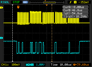
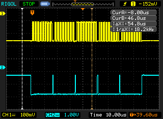
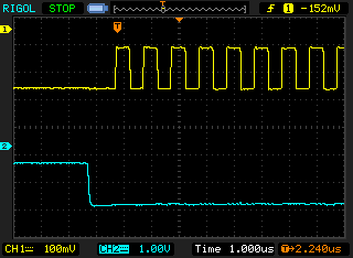
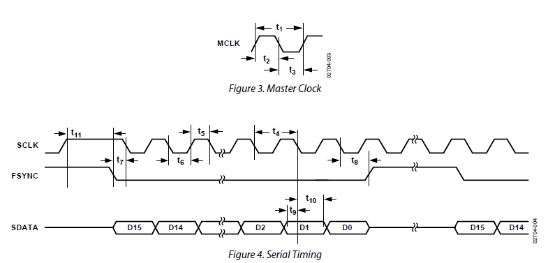
Hi, guys. I just get started using TM4C and I am trying to initialize a function generator chip AD9833. I followed the application notes AN-1070 provided by analog device. These are five sets of data I need write to AD9833 to initialized it, and it should give me a 400Hz sine wave out. 

dataTx[0] = 0x2100;
dataTx[1] = 0x50C7;
dataTx[2] = 0x4000;
dataTx[3] = 0xC000;
dataTx[4] = 0x2000;

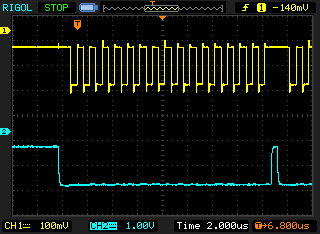
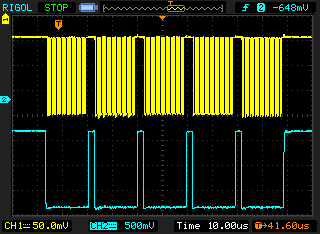
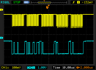
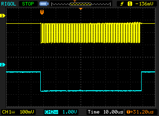
I used UART to test my writing data, it is correct, but the AD9833 doesn't give me any output. Here is my code, hope someone can give me some advice where things might go wrong. I just modified a SPI code from online.

/*
* main.c
*/

// SPI
#define PIN_SSI_CLK GPIO_PIN_4
#define PIN_SSI_FSS GPIO_PIN_5
#define PIN_SSI_TX GPIO_PIN_7
#define GPIO_SSI_BASE GPIO_PORTB_BASE

#include <stdint.h>
#include <stdbool.h>

#include "inc/hw_memmap.h"
#include "inc/hw_ssi.h"
#include "inc/hw_types.h"
#include "driverlib/ssi.h"
#include "driverlib/gpio.h"
#include "driverlib/pin_map.h"
#include "driverlib/sysctl.h"
#include "utils/uartstdio.h"


int main(void) {

uint32_t dataTx[5];
uint32_t index;

// configure clock
SysCtlClockSet(SYSCTL_SYSDIV_1 | SYSCTL_USE_PLL |SYSCTL_USE_OSC | SYSCTL_OSC_MAIN | SYSCTL_XTAL_16MHZ);

// configure SPI 2 on GPIO Port B
SysCtlPeripheralEnable(SYSCTL_PERIPH_SSI2);
SysCtlPeripheralEnable(SYSCTL_PERIPH_GPIOB);

// configure SPI 2
GPIOPinConfigure(GPIO_PB4_SSI2CLK);
GPIOPinConfigure(GPIO_PB5_SSI2FSS);
GPIOPinConfigure(GPIO_PB6_SSI2RX);
GPIOPinConfigure(GPIO_PB7_SSI2TX);
GPIOPinTypeSSI(GPIO_SSI_BASE,PIN_SSI_CLK |PIN_SSI_FSS |PIN_SSI_TX);

// enable SPI 2
SSIConfigSetExpClk(SSI2_BASE, SysCtlClockGet(), SSI_FRF_MOTO_MODE_0, SSI_MODE_MASTER, 1000000, 16);
SSIEnable(SSI2_BASE);

// initialize data
dataTx[0] = 0x2100;
dataTx[1] = 0x50C7;
dataTx[2] = 0x4000;
dataTx[3] = 0xC000;
dataTx[4] = 0x2000;

for(index = 0; index < 5; index++){
SSIDataPut(SSI2_BASE, dataTx[index]);
}
while(SSIBusy(SSI2_BASE)) // waiting if data is sent
{
}

while(1)
{

}

}

  • Hello Jingyuan,

    First of all the function call

    SysCtlClockSet(SYSCTL_SYSDIV_1 | SYSCTL_USE_PLL |SYSCTL_USE_OSC | SYSCTL_OSC_MAIN | SYSCTL_XTAL_16MHZ);

    is incorrect. You are mentioning both USE_PLL and USE_OSC. Only one of them must be used.

    Secondly, can you check the SSI2 Registers to see if the dividers, bit width and mode are correctly configured

    Thirdly if all checks pass, connect a scope probe on the CLK, FSS and TX and see if the data is coming out. Also note that even though you are not using SSI2RX pin, it is good to flush the RXFIFO (to avoid later surprises)

    Regards
    Amit
  • Agree w/Amit's findings & especially with the direction to, 'Fly less blind" by monitoring the MCU's select outputs.

    Our small tech firm has advised clients (successfully) seeking to use that exact device - we know it to mate & play nicely w/this vendor's MCUs.

    We hope that you have an "official" AD eval board - they're not priced too bad - and there have been reports of "lesser boards" using "counterfeit" devices or improper implementation.

    While you & Amit mention the necessary MCU SPI signals - does not another - critical to this DDS chip's operation - remain silent?   (that would be MCLK - appearing upon pin 5 of this 10 pin device)    How have you treated (i.e. provided for/driven) this pin?    (note: some - but not all - Eval boards manage this pin - thus the importance of an official - not cost-down board - from "unknown" source...)

    Note further that all data is clocked in on SPI clock's negative edge and a 16 bit data stream - w/FSync held low throughout - is required...

  • Hi Amit,

    Thank you for your suggestions!

    I changed your first problem. For second problem I don't think it matters because I tried all four different mode 0,1,2,3. They all give me the same thing-no output. Below are my screen shots showing SCLK, SDATA, FSYNC timing diagram. I only have two channel, so first plot is SCLK + SDATA, and the second is SCLK + FSYNC. In my view they all look correct. The third plot is a starting condition (SCLK + FSYNC). By doing this, I put the sending for loop inside of a while(1) loop just for continuously showing waveform, but for the AD9833 initialization, this five sets of data only needs to be written once (outside of while(1) loop). 

    There are five sets of SCLK signal. Channel 2 is my SDATA, and it is the data I wrote in my program. 

    Channel 2 is te FSYNC, as it should be, it is only pulled to high in between of two sets. 


    This one shows the starting condition, which I am not quite sure it is right. In figure 4, which is the timing diagram from AD9833 datasheet. t11 is at high, but in my screenshots, SCLK starts from low. I am not sure whether this is the point. 

  • Hi,
    I bought the AD9833 module from eBay, and I tested it out on my arduino board using some online code. It works not perfectly, but fine. So I think the evaluation board should be good. I replied Amit previously. You can see my screenshots above. I think I am getting correct data out, but for some reason AD9833 doesn't give me any output.
  • Hello Jingyuan,

    Yes, even the data sheet for AD9833 mentions that explicitily. You may have to use SSI_FRF_MOTO_MODE_3 instead of the SSI_FRF_MOTO_MODE_0 in the SSI Controller.

    Regards
    Amit
  • I changed SSI_FRF_MOTO_MODE_2 to mode 2. Although it looks like satisfies the starting condition, I still can't get any output. 

  • Hi Amit,
    I changed it to mode 3, but I am still not getting any output.
  • Hello Jingyuan,

    What is the connection for the other pins of AD9833 device?

    Regards
    Amit
  • Hi Amit, 

    There is a REF, which I didn't use. Others are SCLK, SDATA, FNC,GND,VCC,OUT. 

  • I tested it on my arduino board yesterday with the same connect using some online source code and it can output me an sine wave. So I think the connect should be fine.
  • Hello Jingyuan,

    Can you check the waveform for Mode-3? I think the FSS is not toggling between the words. If that indeed is the case, then change the program as and send an updated plot.

    for(index = 0; index < 5; index++){
    SSIDataPut(SSI2_BASE, dataTx[index]);
    while(SSIBusy(SSI2_BASE));
    }

    Regards
    Amit
  • Hi Amit,

    Here are my updated program and waveform for mode 3:

    int main(void) {

    uint32_t dataTx[5];
    uint32_t dataRx[5];
    uint32_t index;

    // configure clock
    SysCtlClockSet(SYSCTL_SYSDIV_1 |SYSCTL_USE_OSC | SYSCTL_OSC_MAIN| SYSCTL_XTAL_16MHZ );

    // configure SPI 2 on GPIO Port B
    SysCtlPeripheralEnable(SYSCTL_PERIPH_SSI2);
    SysCtlPeripheralEnable(SYSCTL_PERIPH_GPIOB);

    // configure SPI 2
    GPIOPinConfigure(GPIO_PB4_SSI2CLK);
    GPIOPinConfigure(GPIO_PB5_SSI2FSS);
    GPIOPinConfigure(GPIO_PB6_SSI2RX);
    GPIOPinConfigure(GPIO_PB7_SSI2TX);
    GPIOPinTypeSSI(GPIO_SSI_BASE,PIN_SSI_CLK |PIN_SSI_FSS |PIN_SSI_RX |PIN_SSI_TX);

    // enable SPI 2
    SSIConfigSetExpClk(SSI2_BASE, SysCtlClockGet(), SSI_FRF_MOTO_MODE_3, SSI_MODE_MASTER, 1000000, 16);
    SSIEnable(SSI2_BASE);

    // initialize data
    dataTx[0] = 0x2100;
    dataTx[1] = 0x50C7;
    dataTx[2] = 0x4000;
    dataTx[3] = 0xC000;
    dataTx[4] = 0x2000;

    while(1){
    for(index = 0; index < 5; index++){
    SSIDataPut(SSI2_BASE, dataTx[index]);
    while(SSIBusy(SSI2_BASE));
    }
    //while(SSIBusy(SSI2_BASE)) // waiting if data is sent
    //{
    //}

    SysCtlDelay(1000);
    //while(1)
    //{

    }

    }

    Below is the plot of SCLK + FSYNC

    Below is the plot of SCLK + SDATA, which looks wrong comparing to the data I want to write. 

    If I change the while(SSIBusy(SSI2_BASE)); back to outside of the for loop, which is:

    for(index = 0; index < 5; index++){
    SSIDataPut(SSI2_BASE, dataTx[index]);
    //while(SSIBusy(SSI2_BASE));
    }
    while(SSIBusy(SSI2_BASE)); // waiting if data is sent
    //{
    //}

    it gives me the SCLK + FSYNC waveform of:

    No matter how I change mode and position of while(SSIBusy(SSI2_BASE)); there is still no output.

  • Hello Jingyuan

    Why is the Data wrong when compared to the data you want to write in the 2nd plot? Also you would need to put in the SSIBusy condition as only then will you have 5 distinct transfers while toggling FSYNC

    Regards
    Amit
  • Hi Amit,
    The data is wrong in second plot, if you go back to where I sent you SDATA plot first time. They are different. Then, I don't quite understand what do you mean by "Also you would need to put in the SSIBusy condition as only then will you have 5 distinct transfers while toggling FSYNC". Does that mean SSIBusy condition should appear where I finished sending all five words, which is the outside of that for loop?
  • In short, if I put SSIBusy condition inside of the for loop, it gives me the wrong SDATA. If I put SSIBusy condition outside of the for loop, it gives me the correct SDATA.
  • Hello Jingyuan,

    Please read the data sheet for the different modes of SSI especially the section for continuous transfers. Note that what you are interpreting as wrong data is during the time FSYNC is high and must be ignored by the slave device (unless the slave device really care what is there on the data bus when FSYNC is high)

    To test the theory, I would suggest using a bit banging of the GPIO pins to emulate the SSI protocol and then see if you can get the correct waveform of AD9833 device.

    Regards
    Amit