This thread has been locked.

If you have a related question, please click the "Ask a related question" button in the top right corner. The newly created question will be automatically linked to this question.

ADC Trigger using External GPIO

I recently finished the Edx course - "Embedded Systems - shape the world", although I have to confess my understanding of the embedded world is still partial, though my spirit to execute and will to learn is on an all time high :). 

I am trying to build a circuit for our instrumentation application which uses the ADC. The difference between the provided example and my requirement is : I want to trigger the ADC using external GPIO like a switch press (which would be implemented by inserting a push-button between any GPIO pin and GND). 

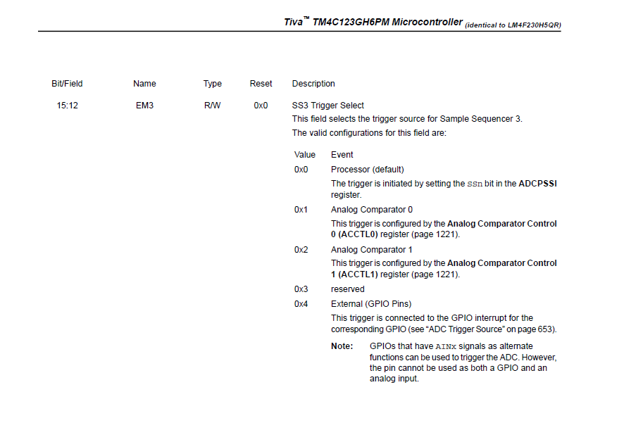
Upon reading a little of datasheet etc. I found this - the register responsible for this is : ADC Event Multiplexer Select (ADCEMUX), (Pg - 830, TM4C123G - TIVA Launchpad), where external triggers can be set by setting the bits 12:15 to 0x4.


Although I am stumped about how to proceed further. What other changes have to be made to this code of ADC as in the course that interfaces a slide potentiometer to the launchpad and uses software trigger?

  • Hello Chintan,

    1. You need to configure a GPIO to be able to generate the ADC Trigger. Details in the GPIO chapter of the data sheet
    2. Configure the EMUX to accept the trigger from GPIO
    3. Ensure that when a push button is used, there is a good de-bounce circuit. Otherwise you would end up generating multiple triggers.

    Regards
    Amit
  • Hi Amit,

    Wonderful that you added that, "Debounce" caution.

    This catches so many by surprise - concept of switch "bounce" really is hard to fathom.    When this "mystery" rides along with the complexity of the MCU's ADC - results are too often an "adventure."

    Debounce circuit Amit mentions may be all in SW - or all in hardware (resistor & capacitor) or a combination of the two...

  • Hello cb1,

    Not for the ADC or DMA Trigger. These are generated by edges.

    Regards
    Amit
  • Amit Ashara said:
    Ensure that when a push button is used, there is a good de-bounce circuit

    Hi Amit,

    As you may note - I was "tail-chaining" your mention of "debounce."

    I had not intended to limit such "debounce" to any narrowly "triggered" application - simply further describe the usual means to achieve it...

  • Hello cb1

    Point duly noted.

    Regards
    Amit
  • So, I am on my way to implement the steps you outlined.

    Here it goes, in steps:    ( I plan to use PE1 as my GPIO Pin that generates the interrupt)

    1. Set the clock for Port E.   SYSCTL_RCGC2_R |= 0x00000010; (It is already getting set as I am using PE2 for ADC input)

    2. Disable analog function of PE1:   GPIO_PORTE_AMSEL_R  &=  ~0x02;   ( I hope this is friendly, as I am also enabling analog function on PE2                                                                                                                                                                          GPIO_PORTE_AMSEL_R |= 0x04;)

    3. PCTL :    ???? - I am drawing a blank here, having read the datasheet a few times, I am not able to make out what to set the PCTL to ?

    4. DIR: GPIO_PORTE_DIR_R &= ~0x02;     // making PE1 an input

    5. AFSEL:  GPIO_PORTE_AFSEL_R |= 0x02;    // enable alternate function on PE1

    6. DEN:  GPIO_PORTE_DEN_R |= 0x02;        // enable digital I/O on PE1

    /// ADC Trigger specific steps

    7.  GPIOADCCTL:  GPIO_PORTE_ADCCTL_R |= 0x02;     // setting the pin to trigger ADC

    8. GPIOIM:  GPIO_PORTE_IM_R |= 0x02;      // configured as a non-masked interrupt

    9. ADCEMUX:  ADC0_EMUX_R |= 0x4000;    // selecting external GPIO as trigger mechanism, 0x4000, as sample sequencer EM3 is used, - this value in place                                                                                        //     of ADC0_EMUX_R &= ~0xF000;       where software trigger is used.

    The trigger specific steps are derived from your suggestions and datasheet page 653 - inserted

    Finally, about debouncing, I read a little, and found it a little advanced. The simplest solution on little research seemed like this h/w + s/w solution for arduino which might be portable to TIVA C.

    Is the above solution for debouncing feasible / suggested ?

    Kindly forgive silly mistakes in the code above if any and provide feedback and venues of improvement, as this is my first attempt at solving a real problem :)

    Thanks all.

  • Perhaps the (silliest) mistake is your (exclusive) use of the overly complex - (Hard for you, Amit, and we outsiders to understand) Direct Register Macros to program.

    This vendor has an extensive API - rich with example programs - and far easier for, "You, Amit, outsiders" to read/review...
  • Your reference has no HW debouncing and SW will be on no use if you are triggering the A/D directly.

    Debouncing circuits come in varying degrees of covering most cases.

    Figure 3 shows a circuit Ganssle1 suggests. The IC should be a Schmitt trigger inverter, I usually use a 74HCT14 myself for this kind of circuit.

    Robert

    1 - See http://www.ganssle.com/debouncing.htm The circuit is on the second page. The first deals with why it is such a hard problem to solve in general. The data is rather illuminating.

  • @cb1 : This is approach we were taught in class, and I find it quite in sync with the datasheet. 

    Nonetheless, I can imagine various approaches to coding, and to further verify that I am doing everything where it should be, I uploaded the code to a github repo

    Please open it alongside, and you will see file descriptions in the readme, and comments in the code. 

    Specifically, I request you look at the files : ADC_ExternalTrigger.c and file ADC_MainUART.c where in the first file, I define the functions for ADC and triggering and in the later, the main program for ADC. 

    Comments in the code, show the places that I have made change to the original code, which used software trigger. 

    However, if this coding approach is still not peer-friendly, then kindly show me an example of how it should be done, and I will update the code in a jiffy :). 

    @ Robert : I think I will come to debouncing, once I get this to work. 

  • Chintan Pathak4 said:
    kindly show me an example of how it should be done,

    My friend - while you've responded in some detail - there's no mention of:

    a) DRM (Direct Register) coding method which you employed exclusively (which forces great and extensive extra effort upon all "helpers".)

    b) API - you appear either unaware (at worst) or inadequately aware (at best) of the power, precision, speed-up and the significant EASE which results from API use.

    Application programs have been written by experts - free you (and helpers, and Amit) from the necessity to "crank open the MCU manual" and fixate upon the many registers - to include key/critical (often not well highlighted) command/control bits.   Miss just one of these critical bits - your program may fault - or stumble - or worst of all: "appear to work!"

    Along with having been conceived, designed & implemented by "experts" - the API example codings have, "passed the test of time" - have been used (successfully) by thousands!   Can the same be said for your DRM codings?   Is it "ideal" for you to enforce extra time & intense effort upon your "helpers?"

    Might it be proper to ask, "Why such, "Slowed, inefficient, error-prone" approach was taught in your class?   As (successful) small tech biz owner (took past tech firm public) I would never allow staff to, "Slow, Unduly Complicate, & Welcome a potentially error-laden coding approach!"  

    The API is detailed, extremely extensive and ideal for your (and all others') learning.

    Should not a major goal of education be the, "Search, Discovery, Exercise and Implementation" of "best/brightest" means of Problem Solving?"   

    When will that be taught?   And why - only then?

    Surely one needs (some) awareness of arcane yet critical "command/control" bits - w/in the hundreds of MCU Registers.   Yet - when, "great, focused, expert efforts" have already been extended in that objective - is it wise to reject them?     And - to (apparently) be unaware of the API's great utility - even existence?

    In stark contrast - API usage insures all such, "arcane, critical (sometimes unclear) Register bit-banging" is (essentially) done (correctly) for you!   (SO good that!)  

    Might this allow (more) time for your serious review of the reach, power, and proper application of this rich API resource?    Then - might you (really) start solving "real world" MCU application problems - become sensitive to the determination of, "which API segment & function" best serves - and how to effectively deploy this (very real) resource?

    As you wrote atop your very first post - is not the API - rather than DRM - the very best way (and by FAR) - to, "shape the world?"   

  • cb1_mobile said:
    Might it be proper to ask, "Why such, "Slowed, inefficient, error-prone" approach was taught in your class?  

    Probably because they are teaching embedded programming rather than Tiva programming.

    I would argue that such a class should probably spend at least a little time even doing machine language programming (as well as C and assembly language)

    There are multiple reasons for teaching programming at a register level. 

    • Appreciation of how the underlying machinery works (one of the biggest obstacle to efficient debugging/problem solving in embedded software is faulty mental models of how the devices work)
    • Acquisition of low level skills
    • Lack of general availability of TIVA like libraries.  As a note the TIVA series is the first in which I have not written my own register map for the device1. Most micros do not have such a library.  On the few that do the quality tends to range from the poor to the dreadful.  TIVA is the first I've seen I would consider adequate.

    Robert

    1 - I'm still not completely certain that it wouldn't be a good idea to write my own register map. I'll probably not.

  • We must agree then to disagree.    My earlier post today, "e2e.ti.com/.../430847" details my viewpoint.

    While I'm in general agreement w/your points: "appreciation of how underlying works, & ack. of low level skills" the "lack of general availability of libraries" does not hold true for the "market leaders!"   (far from that - in fact)

    The ability to quickly - easily - and with great confidence - REUSE past/previous "known good" code is diluted by the over-use of DRM.   Such convenient, robust "reuse" is vital to small tech firm's success - even survival.     DRM - for the most part - does not meet our (or other firms') requirement for reuse due to the code's obscurity...

    You and I have past agreed upon, "Right Tool for the Job!"    DRM is one tool - its (exclusive) use proves hugely improper as, "right tool!"
  • I think I have reached some kind of solution (using the API), though not without issues.

    Kindly check the code for accuracy and give feedback. Full repo with hardware description. 

    The code samples ADC on PF4 press, but: 

    1. It keeps on sampling as long as the switch is pressed, in place of the desired behavior of one sample per press. 

    2. Sometimes, the ADC samples incorrectly, i.e. gives an older value, if sampled too soon after value changes. 

    #include <stdint.h>
    #include <stdbool.h>
    #include "stdlib.h"
    #include "inc/hw_ints.h"
    #include "inc/hw_memmap.h"
    #include "inc/hw_uart.h"
    #include "inc/hw_gpio.h"
    #include "inc/hw_pwm.h"
    #include "inc/hw_types.h"
    #include "driverlib/adc.h"
    #include "driverlib/timer.h"
    #include "driverlib/gpio.c"
    #include "driverlib/gpio.h"
    #include "driverlib/interrupt.h"
    #include "driverlib/pin_map.h"
    #include "driverlib/rom.h"
    #include "driverlib/rom_map.h"
    #include "driverlib/sysctl.c"
    #include "driverlib/sysctl.h"
    #include "driverlib/uart.h"
    #include "driverlib/udma.h"
    #include "driverlib/pwm.h"
    #include "driverlib/ssi.h"
    #include "driverlib/systick.h"
    #include "driverlib/adc.h"
    #include "utils/uartstdio.h"
    #include "utils/uartstdio.c"
    #include <string.h>
    
    void InitPortE(void);
    //*****************************************************************************
    //
    // This function sets up UART0 to be used for a console to display information
    // as the example is running.
    //
    //*****************************************************************************
    void
    InitConsole(void)
    {
        //
        // Enable GPIO port A which is used for UART0 pins.
        // TODO: change this to whichever GPIO port you are using.
        //
        SysCtlPeripheralEnable(SYSCTL_PERIPH_GPIOA);
    
        //
        // Configure the pin muxing for UART0 functions on port A0 and A1.
        // This step is not necessary if your part does not support pin muxing.
        // TODO: change this to select the port/pin you are using.
        //
        GPIOPinConfigure(GPIO_PA0_U0RX);
        GPIOPinConfigure(GPIO_PA1_U0TX);
    
        //
        // Enable UART0 so that we can configure the clock.
        //
        SysCtlPeripheralEnable(SYSCTL_PERIPH_UART0);
    
        //
        // Use the internal 16MHz oscillator as the UART clock source.
        //
        UARTClockSourceSet(UART0_BASE, UART_CLOCK_PIOSC);
    
        //
        // Select the alternate (UART) function for these pins.
        // TODO: change this to select the port/pin you are using.
        //
        GPIOPinTypeUART(GPIO_PORTA_BASE, GPIO_PIN_0 | GPIO_PIN_1);
    
        //
        // Initialize the UART for console I/O.
        //
        UARTStdioConfig(0, 115200, 16000000);
    }
    
    void InitPortEF(void) {
    	
    	// Enable Port E
    	SysCtlPeripheralEnable(SYSCTL_PERIPH_GPIOE);
    	// Enable Port F
    	SysCtlPeripheralEnable(SYSCTL_PERIPH_GPIOF);
    	// Delay to let the clock stabilise
    	SysCtlDelay(3);
    	
    	// For making PE2 as ADC input pin
    	GPIOPinTypeADC(GPIO_PORTE_BASE, GPIO_PIN_2);
    	
    //	// Making PE1 as trigger for ADC
    //	GPIOADCTriggerEnable(GPIO_PORTE_BASE, GPIO_PIN_1);
    	
    	/*
        Configure the switch on the left of the launchpad, GPIO_PIN_4 to a input with
        internal pull-up.
      */
      GPIOPinTypeGPIOInput(GPIO_PORTF_BASE, GPIO_PIN_4);
      GPIOPadConfigSet(GPIO_PORTF_BASE, GPIO_PIN_4, GPIO_STRENGTH_2MA, GPIO_PIN_TYPE_STD_WPU);
    	
    	// Make PF4 a trigger for ADC
    	GPIOADCTriggerEnable(GPIO_PORTF_BASE, GPIO_PIN_4);
    }
    
    int main(){
    	  SysCtlClockSet(SYSCTL_SYSDIV_2_5|SYSCTL_USE_PLL|SYSCTL_OSC_MAIN|SYSCTL_XTAL_16MHZ);
    	  InitConsole();
    		InitPortEF();
    	    //
    	    // This array is used for storing the data read from the ADC FIFO. 
    	    //
    	    uint32_t ADCValues[1];
    			uint32_t value=0;  // Stores the value from PF4
    	    
    	    //
    	    // Display the setup on the console.
    	    //
    	    UARTprintf("ADC ->\n");
    	    UARTprintf("  Type: Slide Potentiometer\n");
    	    UARTprintf("  Samples: One\n");
    	    UARTprintf("  Updates on PF4 press");
    	    UARTprintf("  Input Pin: PE2\n\n");
    
    	    //
    	    // The ADC0 peripheral must be enabled for use.
    	    //
    	    SysCtlPeripheralEnable(SYSCTL_PERIPH_ADC0);
    	    SysCtlDelay(3);
    
    	    //
    	    // Enable sample sequence 3 with a external signal trigger.  Sequence 3
    	    // will do a single sample when the processor sends a singal to start the
    	    // conversion.  Each ADC module has 4 programmable sequences, sequence 0
    	    // to sequence 3.  This example is arbitrarily using sequence 3.
    	    //
    	    ADCSequenceConfigure(ADC0_BASE, 3, ADC_TRIGGER_EXTERNAL, 0);
    
    	    //
    	    // Configure step 0 on sequence 3.  Sample channel 1 (ADC_CTL_CH1) and configure the interrupt flag (ADC_CTL_IE) to be set
    	    // when the sample is done.  Tell the ADC logic that this is the last
    	    // conversion on sequence 3 (ADC_CTL_END).  
    	    //
    	    ADCSequenceStepConfigure(ADC0_BASE, 3, 0, ADC_CTL_CH1 | ADC_CTL_IE |
    	                             ADC_CTL_END);
    
    	    //
    	    // Since sample sequence 3 is now configured, it must be enabled.
    	    //
    	    ADCSequenceEnable(ADC0_BASE, 3);
    
    	    //
    	    // Clear the interrupt status flag.  This is done to make sure the
    	    // interrupt flag is cleared before we sample.
    	    //
    	    ADCIntClear(ADC0_BASE, 3);
    
    	    //
    	    // Sample the ADC forever.  Display the value on the
    	    // console.
    	    //
    	    while(1)
    	    {
    	        //
    	        // Trigger the ADC conversion.
    	        //
    	        // ADCProcessorTrigger(ADC0_BASE, 3);
    					
    					// Read the PF4 state into value
    	        value = GPIOPinRead(GPIO_PORTF_BASE, GPIO_PIN_4);
    				
    					// If PF4 is pressed, trigger ADC conversion
    				  if(( value & GPIO_PIN_4 )==0) {
    							//
    							// Wait for conversion to be completed.
    							//
    							while(!ADCIntStatus(ADC0_BASE, 3, false))
    							{
    							}
    
    							//
    							// Clear the ADC interrupt flag.
    							//
    							ADCIntClear(ADC0_BASE, 3);
    
    							//
    							// Read ADC Value.
    							//
    							ADCSequenceDataGet(ADC0_BASE, 3, ADCValues);
    												
    							//
    							// Display the ADCValue on the console.
    							//
    							UARTprintf("ADC VALUE: %4d\r", ADCValues[0]);
    							
    							// A rude way to avoid bouncing
    							SysCtlDelay(7000000);
    						
    					}
    	        
    	    }
    }

  • Pending debouncing issues ofcourse.
  • Chintan Pathak4 said:
    Pending debouncing issues ofcourse.

    Debounce most always confounds new users - it so often is "outside" of user expectations.    (i.e. how possibly could a mechanical switch "bounce?")   (scope across the switch contacts - quickly reveals the extent of such bounce)

    Robert provided a neat debounce circuit.    Another - time tested - is the cmos 555 timer IC - set up in "one-shot" mode.    Output is pure - even if the input to the 555 "bounces."  (assumes the one shot's duration exceeds that of the switch bounce)

    May I applaud your "admittance" of some API usage to speed, ease & enhance your learning.   As the API functions have far more descriptive names - and usually impact fewer MCU register bits - some, "self commenting" is afforded.    Yet still you should comment as to your intent w/any function which is not "obvious."

    I hope my point re: the total obscurity of your (hopefully past) "uncommented DRM coding" has registered - and been accepted.    Again - you really cannot bring that cryptic code barrage to a senior co-worker (as you've done here) and expect assistance/sympathy!    

    The likelihood that "so many" bits are controlled by a single DRM code line does require great time, focus & effort to "get right" - yet the absence of comments creates essentially, "unreadable code which is not suitable for reuse" without a serious "page by page re-read of the trusty MCU manual" and each every code line (again) test/verified.   How can that make sense?

    Again I come from the small tech biz viewpoint (likely employers of so many, here) [and "why" I'm here] - talk to many such biz owners - none would trade the, "Speed, efficiency & correctness" of the API for our "new hires" use of DRM - so that they can really "learn."    (suspect the "learning" from that method is, "How fast can we kill development - Shut the doors?")    Excelsior...


  • Hello Chintan

    Configure the GPIO Pin to be a falling edge triggered if you want one sample per Switch press. That should help avoid the issue of Key Press causing multiple samples (unless that is what you intent to)

    Regards
    Amit
  • You do want to take of the debounce but that is a separate issue from your always running the A/D when the switch is on.

    What you want to do in that case is change from your current level trigger (always converting when the switch is "on") to and edge trigger.

    The trigger becomes sample once when the switch goes "on" then go into an idle until it goes off. Basically a small state machine. This is where the effects of bounce will really show up.

    Robert

    I do have a pointer to a possible state machine editor if you are interested.
  • @Robert - Would love to see the state machine editor you refer to. 

    I found this code  and this. Both talk about setting a GPIO interrupt with Falling edge etc. and have similar steps like 

    GPIOIntRegister(GPIO_PORTF_BASE, onButtonUp);   // Register our handler function for port F
    GPIOIntTypeSet(GPIO_PORTF_BASE, GPIO_PIN_4, GPIO_RISING_EDGE);          // Configure PF4 for rising edge trigger
    GPIOIntClear(GPIO_PORTF_BASE, GPIO_PIN_4);  // Clear interrupt flag

    Now, I am wondering, if I set my GPIO pin as an interrrupt alongwith an input, then would it not conflict with 

    	// Make PF4 a trigger for ADC
    	GPIOADCTriggerEnable(GPIO_PORTF_BASE, GPIO_PIN_4);

    this is how I make the GPIO to trigger the ADC. 

    @cb1: So the problems with API (aka encapsulation) are apparent here. All their effects are not documented, so what happens inside the function call, exactly what registers are changed is a mystery and is left to either the user's interpretation or trial and error. 

  • Chintan Pathak4 said:
    @cb1: So the problems with API (aka encapsulation) are apparent here. All their effects are not documented

    Your word-picture here is (almost) perfect - but for your mistaken use of "API" when you (clearly) meant DRM!   (attention to such detail - is required)

    Nothing prevents you - once the use of the API enables you to quickly, easily & correctly meet your program goal - from reviewing the API's source code - and (then) digging deep.  (into the always interesting - Register bit constructs...)

    Yet - and critically - you've not had to post here - or torment senior co-workers - who will not take kindly to having to "delve into" a barrage of uncommented, overly-cryptic - non-reusable code...

  • Hello Chintan,

    The ADC Trigger is based on the condition set for the Interrupt. The interrupt condition decides the qualifier which is then used for ADC and DMA Trigger.

    Regards
    Amit
  • Thanks all,

    I reached the solution due to the respected members nurturing.

    Final solution up for review, (as well commented as I could)

    // This code makes the TM4C123GXL Tiva-C launchpad
    // sample an ADC value, upon an external trigger
    
    // Slide Potentiometer connected on PE2
    // Trigger generated on PF4
    // ADC Value sent to UART, once per ButtonDown


    // #define PART_TM4C123GH6PM
    
    #include <stdint.h>
    #include <stdbool.h>
    #include "stdlib.h"
    #include "inc/hw_ints.h"
    #include "inc/hw_memmap.h"
    #include "inc/hw_uart.h"
    #include "inc/hw_gpio.h"
    #include "inc/hw_pwm.h"
    #include "inc/hw_types.h"
    #include "driverlib/adc.h"
    #include "driverlib/timer.h"
    #include "driverlib/gpio.c"
    #include "driverlib/gpio.h"
    #include "driverlib/interrupt.h"
    #include "driverlib/pin_map.h"
    #include "driverlib/rom.h"
    #include "driverlib/rom_map.h"
    #include "driverlib/sysctl.c"
    #include "driverlib/sysctl.h"
    #include "driverlib/uart.h"
    #include "driverlib/udma.h"
    #include "driverlib/pwm.h"
    #include "driverlib/ssi.h"
    #include "driverlib/systick.h"
    #include "driverlib/adc.h"
    #include "utils/uartstdio.h"
    #include "utils/uartstdio.c"
    #include <string.h>
    
    void InitPortEF(void);      // Function to initialise Port E and Port F
    
    //volatile uint32_t value=0;  // global variable - Stores the value from PF4
    //*****************************************************************************
    //
    // This function sets up UART0 to be used for a console to display information
    // as the example is running.
    //
    //*****************************************************************************
    void
    InitConsole(void)
    {
        //
        // Enable GPIO port A which is used for UART0 pins.
        // TODO: change this to whichever GPIO port you are using.
        //
        SysCtlPeripheralEnable(SYSCTL_PERIPH_GPIOA);
    
        //
        // Configure the pin muxing for UART0 functions on port A0 and A1.
        // This step is not necessary if your part does not support pin muxing.
        // TODO: change this to select the port/pin you are using.
        //
        GPIOPinConfigure(GPIO_PA0_U0RX);
        GPIOPinConfigure(GPIO_PA1_U0TX);
    
        //
        // Enable UART0 so that we can configure the clock.
        //
        SysCtlPeripheralEnable(SYSCTL_PERIPH_UART0);
    
        //
        // Use the internal 16MHz oscillator as the UART clock source.
        //
        UARTClockSourceSet(UART0_BASE, UART_CLOCK_PIOSC);
    
        //
        // Select the alternate (UART) function for these pins.
        // TODO: change this to select the port/pin you are using.
        //
        GPIOPinTypeUART(GPIO_PORTA_BASE, GPIO_PIN_0 | GPIO_PIN_1);
    
        //
        // Initialize the UART for console I/O.
        //
        UARTStdioConfig(0, 115200, 16000000);
    }
    
    void InitPortEF(void) {
    	
    	// Enable Port E
    	SysCtlPeripheralEnable(SYSCTL_PERIPH_GPIOE);
    	// Enable Port F
    	SysCtlPeripheralEnable(SYSCTL_PERIPH_GPIOF);
    	// Delay to let the clock stabilise
    	SysCtlDelay(3);
    	
    	// For making PE2 as ADC input pin
    	GPIOPinTypeADC(GPIO_PORTE_BASE, GPIO_PIN_2);
    	
    	/*
        Configure the switch on the left of the launchpad, GPIO_PIN_4 to a input with
        internal pull-up.
      */
      GPIOPinTypeGPIOInput(GPIO_PORTF_BASE, GPIO_PIN_4);
      GPIOPadConfigSet(GPIO_PORTF_BASE, GPIO_PIN_4, GPIO_STRENGTH_2MA, GPIO_PIN_TYPE_STD_WPU);
    	GPIOIntTypeSet(GPIO_PORTF_BASE,GPIO_PIN_4,GPIO_FALLING_EDGE);
    	// Make PF4 a trigger for ADC
    	GPIOADCTriggerEnable(GPIO_PORTF_BASE, GPIO_PIN_4);
    }
    
    int main(){
    	  SysCtlClockSet(SYSCTL_SYSDIV_2_5|SYSCTL_USE_PLL|SYSCTL_OSC_MAIN|SYSCTL_XTAL_16MHZ);
    	  InitConsole();
    		InitPortEF();
    	    //
    	    // This array is used for storing the data read from the ADC FIFO. It
    	    // must be as large as the FIFO for the sequencer in use.  This example
    	    // uses sequence 3 which has a FIFO depth of 1.  If another sequence
    	    // was used with a deeper FIFO, then the array size must be changed.
    	    //
    	    uint32_t ADCValues[1];
    			uint32_t value=0;  // Stores the value from PF4
    	    
    	    //
    	    // Display the setup on the console.
    	    //
    	    UARTprintf("ADC ->\n");
    	    UARTprintf("  Type: Slide Potentiometer\n");
    	    UARTprintf("  Samples: One\n");
    	    UARTprintf("  Updates on PF4 press");
    	    UARTprintf("  Input Pin: PE2\n\n");
    
    	    //
    	    // The ADC0 peripheral must be enabled for use.
    	    //
    	    SysCtlPeripheralEnable(SYSCTL_PERIPH_ADC0);
    	    SysCtlDelay(3);
    
    	    //
    	    // Enable sample sequence 3 with a external signal trigger.  Sequence 3
    	    // will do a single sample when the processor sends a singal to start the
    	    // conversion.  Each ADC module has 4 programmable sequences, sequence 0
    	    // to sequence 3.  This example is arbitrarily using sequence 3.
    	    //
    	    ADCSequenceConfigure(ADC0_BASE, 3, ADC_TRIGGER_EXTERNAL, 0);
    
    	    //
    	    // Configure step 0 on sequence 3.  Sample channel 1 (ADC_CTL_CH1) and configure the interrupt flag (ADC_CTL_IE) to be set
    	    // when the sample is done.  Tell the ADC logic that this is the last
    	    // conversion on sequence 3 (ADC_CTL_END).  Sequence 3 has only one
    	    // programmable step.  Sequence 1 and 2 have 4 steps, and sequence 0 has
    	    // 8 programmable steps.  Since we are only doing a single conversion using
    	    // sequence 3 we will only configure step 0.  For more information on the
    	    // ADC sequences and steps, reference the datasheet.
    	    //
    	    ADCSequenceStepConfigure(ADC0_BASE, 3, 0, ADC_CTL_CH1 | ADC_CTL_IE |
    	                             ADC_CTL_END);
    
    	    //
    	    // Since sample sequence 3 is now configured, it must be enabled.
    	    //
    	    ADCSequenceEnable(ADC0_BASE, 3);
    
    	    //
    	    // Clear the interrupt status flag.  This is done to make sure the
    	    // interrupt flag is cleared before we sample.
    	    //
    	    ADCIntClear(ADC0_BASE, 3);
    
    	    //
    	    // Sample the ADC forever.  Display the value on the
    	    // console.
    	    //
    	    while(1)
    	    {
    				  SysCtlDelay(7000000);
    	        //
    	        // Trigger the ADC conversion.
    	        //
    	        // ADCProcessorTrigger(ADC0_BASE, 3);
    					
    					// Read the PF4 state into value
    	        value = GPIOPinRead(GPIO_PORTF_BASE, GPIO_PIN_4);
    				
    					// If PF4 is pressed, trigger ADC conversion
    				  if(( value & GPIO_PIN_4 )==0) {
    							//
    							// Wait for conversion to be completed.
    							//
    							while(!ADCIntStatus(ADC0_BASE, 3, false))
    							{
    							}
    
    							//
    							// Clear the ADC interrupt flag.
    							//
    							ADCIntClear(ADC0_BASE, 3);
    
    							//
    							// Read ADC Value.
    							//
    							ADCSequenceDataGet(ADC0_BASE, 3, ADCValues);
    												
    							//
    							// Display the ADCValue on the console.
    							//
    							UARTprintf("ADC VALUE: %4d\r", ADCValues[0]);
    							
    							// A rude way to avoid bouncing
    							SysCtlDelay(7000000);
    						
    					}
    	        //
    	        // This function provides a means of generating a constant length
    	        // delay.  The function delay (in cycles) = 3 * parameter.  Delay
    	        // 250ms arbitrarily.
    	        //
    	        //SysCtlDelay(80000000 / 12);
    	    }
    }
    

    If everything is fine, I will mark all the posts by Amit as answers

  • Even senior programmers (my small tech shop) would welcome your "hire or interning" NOW! (as the code - essentially DRM-Free - and commented - and so understandable by virtue of the API's clever function naming - is so much clearer - and vastly more, "reusable.")

    One "green tick" for "KILL uncommented DRM" among the "sea of green" for Amit - could not hurt...  (and really will, "shape the world.")