This thread has been locked.

If you have a related question, please click the "Ask a related question" button in the top right corner. The newly created question will be automatically linked to this question.

Custom board debug advice

Other Parts Discussed in Thread: TM4C129XNCZAD, UNIFLASH

Hello,

I have 2 custom make PCB that built with brand new tm4c129xnczad. The problem is both boards fail to connect to JTAG by using DK-TM4C123G evaluation board as debugger. I think DK-TM4C123G debugger is working as it can be used to connect to another boards.

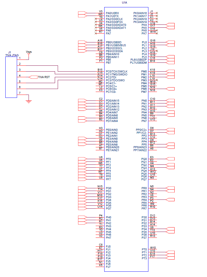
The schematic design of the custom board is based on DK-TM4C129X. The exception is no 32.768KHz crystal, Ethernet pins are NC, HIB is NC, Wake pin is pull-high. I believe the above differences should not make the JTAG connection fail. In additional to CCS, I have tried to use Uniflash program, Unlock procedure, slower JTAG clock rate, but do not help.

Any debug idea is welcome.

Thanks,

Benson

  • More information about the boards - 25MHz crystal is running, VDDC is 1.2V. Current is 28mA normally, 15mA when reset pin is held.
  • I probably cannot help you but if you can post an image of your JTAG circuit it might help others help you. There are sometimes subtle points in that that are missed.

    Robert
  • Tried to use another debugger (XDS100v3), seems the JTAG connection is OK.

    But still fail to connect to the target.

    Error connecting to the target "Error -2062"


    The following is the target test connection log.

    [Start: Texas Instruments XDS100v3 USB Debug Probe_0]

    Execute the command:

    %ccs_base%/common/uscif/dbgjtag -f %boarddatafile% -rv -o -F inform,logfile=yes -S pathlength -S integrity

    [Result]

    -----[Print the board config pathname(s)]------------------------------------

    C:\Users\BENSON~1\AppData\Local\TEXASI~1\

       CCS\ti\0\0\BrdDat\testBoard.dat

    -----[Print the reset-command software log-file]-----------------------------

    This utility has selected a 100- or 510-class product.

    This utility will load the adapter 'jioserdesusbv3.dll'.

    The library build date was 'Feb 18 2015'.

    The library build time was '23:56:50'.

    The library package version is '5.1.641.0'.

    The library component version is '35.34.40.0'.

    The controller does not use a programmable FPGA.

    The controller has a version number of '4' (0x00000004).

    The controller has an insertion length of '0' (0x00000000).

    This utility will attempt to reset the controller.

    This utility has successfully reset the controller.

    -----[Print the reset-command hardware log-file]-----------------------------

    The scan-path will be reset by toggling the JTAG TRST signal.

    The controller is the FTDI FT2232 with USB interface.

    The link from controller to target is direct (without cable).

    The software is configured for FTDI FT2232 features.

    The controller cannot monitor the value on the EMU[0] pin.

    The controller cannot monitor the value on the EMU[1] pin.

    The controller cannot control the timing on output pins.

    The controller cannot control the timing on input pins.

    The scan-path link-delay has been set to exactly '0' (0x0000).

    -----[The log-file for the JTAG TCLK output generated from the PLL]----------

     Test  Size   Coord      MHz    Flag  Result       Description

     ~~~~  ~~~~  ~~~~~~~  ~~~~~~~~  ~~~~  ~~~~~~~~~~~  ~~~~~~~~~~~~~~~~~~~

       1    512  - 01 00  500.0kHz   O    good value   measure path length

       2    512  + 01 20  3.000MHz  [O]   good value   apply explicit tclk

    There is no hardware for measuring the JTAG TCLK frequency.

    In the scan-path tests:

    The test length was 16384 bits.

    The JTAG IR length was 4 bits.

    The JTAG DR length was 1 bits.

    The IR/DR scan-path tests used 2 frequencies.

    The IR/DR scan-path tests used 500.0kHz as the initial frequency.

    The IR/DR scan-path tests used 3.000MHz as the highest frequency.

    The IR/DR scan-path tests used 3.000MHz as the final frequency.

    -----[Measure the source and frequency of the final JTAG TCLKR input]--------

    There is no hardware for measuring the JTAG TCLK frequency.

    -----[Perform the standard path-length test on the JTAG IR and DR]-----------

    This path-length test uses blocks of 512 32-bit words.

    The test for the JTAG IR instruction path-length succeeded.

    The JTAG IR instruction path-length is 4 bits.

    The test for the JTAG DR bypass path-length succeeded.

    The JTAG DR bypass path-length is 1 bits.

    -----[Perform the Integrity scan-test on the JTAG IR]------------------------

    This test will use blocks of 512 32-bit words.

    This test will be applied just once.

    Do a test using 0xFFFFFFFF.

    Scan tests: 1, skipped: 0, failed: 0

    Do a test using 0x00000000.

    Scan tests: 2, skipped: 0, failed: 0

    Do a test using 0xFE03E0E2.

    Scan tests: 3, skipped: 0, failed: 0

    Do a test using 0x01FC1F1D.

    Scan tests: 4, skipped: 0, failed: 0

    Do a test using 0x5533CCAA.

    Scan tests: 5, skipped: 0, failed: 0

    Do a test using 0xAACC3355.

    Scan tests: 6, skipped: 0, failed: 0

    All of the values were scanned correctly.

    The JTAG IR Integrity scan-test has succeeded.

    -----[Perform the Integrity scan-test on the JTAG DR]------------------------

    This test will use blocks of 512 32-bit words.

    This test will be applied just once.

    Do a test using 0xFFFFFFFF.

    Scan tests: 1, skipped: 0, failed: 0

    Do a test using 0x00000000.

    Scan tests: 2, skipped: 0, failed: 0

    Do a test using 0xFE03E0E2.

    Scan tests: 3, skipped: 0, failed: 0

    Do a test using 0x01FC1F1D.

    Scan tests: 4, skipped: 0, failed: 0

    Do a test using 0x5533CCAA.

    Scan tests: 5, skipped: 0, failed: 0

    Do a test using 0xAACC3355.

    Scan tests: 6, skipped: 0, failed: 0

    All of the values were scanned correctly.

    The JTAG DR Integrity scan-test has succeeded.

    [End: Texas Instruments XDS100v3 USB Debug Probe_0]

  • Hello Benson,

    Can you share the schematics of the TM4C129 part on your board?

    Regards
    Amit
  • Just find something special! Seem related to 25MHz, ROM boot laoder, empty PHY and RBIAS pin...
  • Nicely drawn schematic - good job.

    Here - a few comments:

    a) it is normal/customary to place some capacitor across Reset & ground - minus that "C" your reset may be too brief

    b) critical VRefA+ ties directly to (noisy) VSys.   Note that VRefA+ is brought out separately - so that a better quality voltage (perhaps a precise reference) may be input to VRefA+.   By tieing the (always) noisy VSys - directly to VRefA+ (as your schematic indicates) you have substantially degraded your MCU's Analog performance.

    c) ditto for VRefA- - again this pin should tie to Digital Ground at one point - ideally the "quietest" board ground point.

    d) you've "saved" cost/size of JTAG/SWD pull-up resistors - we find this to so often degrade JTAG signal edges (& levels) - fails miserably at - "Risk-Reward."

    e) power to the MCU board must be proper - and remain such - during any attempt at programming and/or connection.   Is your board supply adequate to task?

  • Benson, what's that JTAG Connector?  I don't recognize it as either the standard 20 pin JTAG connector or the standard ARM Cortex 10 pin connector.  I would suggest staying away from vendor proprietary JTAG connectors.

    cb1_mobile said:
    a) it is normal/customary to place some capacitor across Reset & ground - minus that "C" your reset may be too brief

    Also a series resistor to limit the current when that pin is pulled low by the JTAG. I always use an external supervisory circuit as well.

    cb1_mobile said:
    d) you've "saved" cost/size of JTAG/SWD pull-up resistors - we find this to so often degrade JTAG signal edges (& levels) - fails miserably at - "Risk-Reward."

    Degrade - I've found in practice that this often means does not work.  Always take the most conservative of vendor's evaluation board schematic, ARM's recommendations and vendor's recommendations (and look at the recommendations by the JTAG adapter manufacturers).  It's easy to not populate a resistor, difficult to patch it in later. Resistors are cheap, PCB space for an 0805 resistor is small.

    It's difficult to overemphasize this.

    cb1_mobile said:
    e) power to the MCU board must be proper - and remain such - during any attempt at programming and/or connection.   Is your board supply adequate to task?

    Agreed, use plentiful decoupling, ceramic caps are cheap.

    Robert

  • cb1_mobile said:
    Nicely drawn schematic - good job.

    Yes

    Robert

  • Hello Benson,

    That is what my next question was going to be on. The RBIAS pin is missing in schematic...

    Regards
    Amit