Other Parts Discussed in Thread: EK-TM4C1294XL, EK-TM4C129EXL, ENERGIA
Hello,
I am getting familiar with the EK-TM4C1294XL board, trying to learn some basic things about ARM Cortex-M4 MCUs.
I need some help after having spent the entire day trying to implement SPI on EK-TM4C1294XL board.
I have browsed through several similar topics on this forum and played a little according to the suggestions therein, however without success. That is why I decided to make a new post.
The SPI device is an Analog Devices ADXL362 accelerometer that is mounted on a small breakout PCB. I have used that device sucessfully with a Raspberry Pi in the past.
Connections are as follows: I use the pins of the stacking connectors X6 and X7:
PQ0: SCLK
PQ1: ~CS
PQ2: MOSI
PQ3: MISO
I use Open Bench Logic Sniffer on my laptop PC to spy on the SPI bus. The TiVa evaluation kit runs on my desktop PC.
The code I use is the following:
// InitSPI3() - initialize SPI on SSI3
// Based on code that is available at:
// e2e.ti.com/.../1429666
void
InitSPI3(uint32_t SystemClock, uint32_t SPIMode, uint32_t SPIBitRate)
{
	// The SSI3 peripheral must be enabled for use.
	MAP_SysCtlPeripheralEnable(SYSCTL_PERIPH_SSI3);
	MAP_SysCtlPeripheralEnable(SYSCTL_PERIPH_GPIOQ);

	// Configure the pin muxing for SSI0 functions on port Q0, Q1, Q2, and Q3.
	MAP_GPIOPinConfigure(GPIO_PQ0_SSI3CLK);		// SCLK
	MAP_GPIOPinConfigure(GPIO_PQ1_SSI3FSS);		// ~CS
	MAP_GPIOPinConfigure(GPIO_PQ2_SSI3XDAT0);	// MOSI
	MAP_GPIOPinConfigure(GPIO_PQ3_SSI3XDAT1);	// MISO

	// Configure the GPIO settings for the SSI pins. This function also gives
	// control of these pins to the SSI hardware.
	// The pins are assigned as follows:
	// PQ2 - SSI3Tx
	// PQ3 - SSI3Rx
	// PQ1 - SSI3Fss
	// PQ0 - SSI3CLK
	MAP_GPIOPinTypeSSI(GPIO_PORTQ_BASE, GPIO_PIN_3 | GPIO_PIN_2 | GPIO_PIN_1 | GPIO_PIN_0);

	// Configure and enable the SSI port for SPI MASTER mode.
	MAP_SSIConfigSetExpClk(SSI3_BASE, SystemClock, SPIMode, SSI_MODE_MASTER, SPIBitRate, 8);
	//MAP_SSIAdvModeSet(SSI3_BASE, SSI_ADV_MODE_LEGACY);
	MAP_SSIAdvModeSet(SSI3_BASE, SSI_ADV_MODE_READ_WRITE);
	MAP_SSIAdvFrameHoldEnable(SSI3_BASE);
	MAP_SSIEnable(SSI3_BASE);
}

// used project 'hello' as a base
int
main(void)
{
    ...

    uint32_t ui32ADXL362_ReadDevID[] = {0x0B, 0x00};
    uint8_t i = 0;
    ...

    //
    // Run from the PLL at 120 MHz.
    //
    g_ui32SysClock = MAP_SysCtlClockFreqSet((SYSCTL_XTAL_25MHZ |
                SYSCTL_OSC_MAIN | SYSCTL_USE_PLL |
                SYSCTL_CFG_VCO_480), 120000000);

    //
    // Configure the device pins.
    //
    PinoutSet(false, false);

    ...

	// Initialize the SPI.
	// Settings are compatible with the ADXL362 accelerometer.
	// CPOL=CPHA = 0, f_SCLK, max = 1 MHz
	//
	InitSPI3(g_ui32SysClock, SSI_FRF_MOTO_MODE_0, 500000);
    ...
     SysCtlDelay(1);
     i = 0;
     while(i < 2)
     {
     	SSIDataPutNonBlocking(SSI3_BASE, *(ui32ADXL362_ReadDevID+i++));
     }
     SysCtlDelay(1);

     while(1)
     {
          ...
     }
}
I try to read the Device ID by sending byte sequence 0x0B , 0x00 on the SPI bus. Page 20 of AD's datasheet shows the following waveforms for reading from a single address:
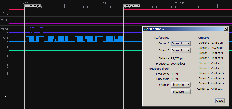
However, what I see on the SPI bus is different:
In InitSPI() function, using:
MAP_SSIAdvModeSet(SSI3_BASE, SSI_ADV_MODE_LEGACY);
results in having the ~CS line going to HIGH between successive byte transfers, which is not the desired case;
and using:
MAP_SSIAdvModeSet(SSI3_BASE, SSI_ADV_MODE_READ_WRITE);
MAP_SSIAdvFrameHoldEnable(SSI3_BASE);
results in the above pattern EXCEPT for the end of transmission; ~CS line does not go to HIGH level . MISO line remains silent:
My question is:
is there any way to implement SPI correctly? What kind of detail am I missing?
I followed a suggestion here and here to use a GPIO pin as ~CS. Here is what I tried, albeit unsuccessfully:
void
InitSPI3(uint32_t SystemClock, uint32_t SPIMode, uint32_t SPIBitRate)
{
	// The SSI3 peripheral must be enabled for use.
	MAP_SysCtlPeripheralEnable(SYSCTL_PERIPH_SSI3);
	MAP_SysCtlPeripheralEnable(SYSCTL_PERIPH_GPIOQ);

	// Configure the pin muxing for SSI0 functions on port Q0, Q1, Q2, and Q3.
	MAP_GPIOPinConfigure(GPIO_PQ0_SSI3CLK);		// SCLK
	//MAP_GPIOPinConfigure(GPIO_PQ1_SSI3FSS);	// ~CS - commented out that line
	MAP_GPIOPinConfigure(GPIO_PQ2_SSI3XDAT0);	// MOSI
	MAP_GPIOPinConfigure(GPIO_PQ3_SSI3XDAT1);	// MISO

	// Configure the GPIO settings for the SSI pins. This function also gives
	// control of these pins to the SSI hardware.
	// The pins are assigned as follows:
 	// PQ2 - SSI3Tx
	// PQ3 - SSI3Rx
	// PQ0 - SSI3CLK
        // Excluding PQ1 from the following function call-will make that a GPIO line
	MAP_GPIOPinTypeSSI(GPIO_PORTQ_BASE, GPIO_PIN_3 | GPIO_PIN_2 | GPIO_PIN_0);

    // rest of function is same as above
}

int
main(void)
{
    uint32_t ui32ADXL362_ReadDevID[] = {0x0B, 0x00};
    uint8_t i = 0;

    //
    // Run from the PLL at 120 MHz.
    //
    g_ui32SysClock = MAP_SysCtlClockFreqSet((SYSCTL_XTAL_25MHZ |
                SYSCTL_OSC_MAIN | SYSCTL_USE_PLL |
                SYSCTL_CFG_VCO_480), 120000000);

    //
    // Configure the device pins.
    //
    PinoutSet(false, false);

   ...

    //
    // Initialize the SPI.
    // Settings are compatible with the ADXL362 accelerometer.
    // CPOL=CPHA = 0, f_SCLK, max = 1 MHz
    //
    InitSPI3(g_ui32SysClock, SSI_FRF_MOTO_MODE_0, 500000);

    // Initalize ~CS as a GPIO pin.
    GPIOPinTypeGPIOOutput(GPIO_PORTQ_BASE, GPIO_PIN_1);

    ...
    GPIOPinWrite(GPIO_PORTQ_BASE, GPIO_PIN_1, 0);
    SysCtlDelay(1);
    i = 0;
    while(i < 2)
    {
    	SSIDataPutNonBlocking(SSI3_BASE, *(ui32ADXL362_ReadDevID+i++));
    }
    SysCtlDelay(1);
    GPIOPinWrite(GPIO_PORTQ_BASE, GPIO_PIN_1, 1);

    ...
}
..?
i need to make this simple thing work, therefore I really count on your kind assistance.