This thread has been locked.

If you have a related question, please click the "Ask a related question" button in the top right corner. The newly created question will be automatically linked to this question.

QSSI-High Speed Clock Operation

Other Parts Discussed in Thread: TM4C1294NCPDT, SN74AVC2T244, LSF0102

Hi

I am using SSI0 module of TM4C1294NCPDT micro controller in freescale legacy mode.

SPI mode used is SPO=0 (Clock polarity low) and SPH=1 (Capture on falling edge).

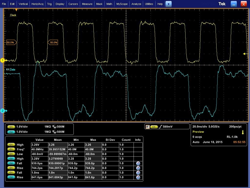
But due to very high propagation delay, RX data from slave looses synchronization with clock. The data is half clock period lagging behind clock.The data captured by MCU is completely different.(Below is the scopeshot captured for RX data with clock on MCU pins).

I have tried to use HSCLKEN bit in the SSI Control 1 (SSICR1) register which datasheet says can be used for faster timing and logic can be used to adjust clock to external data relationships.

But just by setting the HSCLKEN bit is not helping me to solve the problem.

I am not getting much detail in TI documentation on how to implement logic for adjusting clock to external data.

Does anybody have used this feature?

Can anybody help me to solve this problem?

  • Hello Bipin,

    The first thing is the corrective action. Since the propagation delay is very high, you must concentrate your efforts in correcting that using a newer board design.
    You may have to reduce the speed of SSICLK to make it manageable for the design to capture the data

    Just by looking at the scope plot, it is not possible for me to understand what is being sent and what is being captured. Please elaborate.

    Regards
    Amit
  • BIPIN BHATT said:
    due to very high propagation delay, RX data from slave looses synchronization with clock.

    May I agree w/vendor's Amit - that such "high propagation delay" is your - not the MCU's - responsibility.

    That said - would not that same, "high propagation delay" visit your TX data?   If not - might an unwanted capacitance or other component, "sit on that signal trace/MCU pin" - and cause that delay?   As always - would it not prove useful to "swap" that SPI-based IC - with another (fresh) one?

    You've provided no information regarding your MCU board and/or its routing/connection to the flash device.   Long leads, breadboard-like construction & even marginal power levels - any/all may account for the issue you report.

    I'd place much trust in the MCU & Flash vendors  - the implementation/connection between those two - not so much!

  • Hi Amit & Cb1,

    Thanks for reply.
    The propagation delay is caused by level translator SN74AVC2T244. When translating 3.3V logic (MCU) to 1.2V logic.
    Yes the propagation delay is affecting Tx data as well but for that clock is also equally delayed so they are in sync.
    I am just looping back the data by solder shorting Tx with Rx at level translator output.
    I am writing 16-bit data 0xAAAA and receiving the data 0x5555.
    Also by reducing speed to 25MHz, I am able to receive correct data.
    But I am finding a way to take data rate and performance benefit of MCU.

    Regards,
    Bipin
  • BIPIN BHATT said:
    is affecting Tx data as well but for that clock is also equally delayed so they are in sync. 

    As all signals: clock, data (TX & RX), & chip select all must pass through the level translator - I cannot grasp how this impacts RX data alone.   (does not that translator provide, "equal delay" between all signals - which pass thru & are translated?)   [although - there "may" be a direction difference when "up converting" signal levels...i.e. "only" the RX data - which leaves the QSSI @ 1V2 levels - must be, "up converted" (in level)]

    Should that prove the case - I first thought (para just below) - which upon reread I now believe mistaken!

    Should that "direction" result in your propagation delay - cannot you "level shift" (down) the clock - so that it must undergo the same, "up convert" as RX Data?   This may require different circuit configuration so that the level translator presents "identical" delays - in either direction.    (one wonders if a "more equalized" delay device exists - saving you from the effort to "tweak" each signal path...)

    ***Dawns now that the MCU "reads" incoming data on its own clock edge - and there is "nothing" we can do to "delay" that read as it is (likely) routed & handled internally by the MCU.   In this case - I fear that you're "stuck!"

    Might you link to the QSSI data sheet - so that we can determine if, "prop delay" indeed bears such directional "sensitivity."    (stinks if that's true...)

  • Thanks cb1_mobile,

    All signals are passing through level translator and it provides equal delay to all signals. (Not much difference observed while up/down converting.)
    My MCU operates in master mode so it will provide clock and Tx data to level translator and then to the slave device (so they are in sync).
    In reality, slave will send the data with reference to delayed clock.
    The MCU will sampled that Rx data with non-delayed original clock. (so effectively from MCU point of view, Rx data is two times delayed with reference to MCU clock)

    Also I can't get back the delayed version of clock with Rx data and use that clock for capturing data as MCU is master.
    If I use another SSI port in slave mode to get the Rx data with clock then also there is speed limitation in slave mode upto 10MHz.

    Regards,
    Bipin Bhatt
  • That's well answered & explained - thank you - appreciated.

    Agree that when transmitting - and if (indeed) clock & data undergo identical delays - that data should arrive (bit later) but fully, "Sync intact."

    And - as you nicely noted - when operating in "reverse (reading the SPI device) that RX Data may be (almost) 2x delayed.   (I sense that there "might" be some (slight) overlap of the clock's arrival at your QSSI device and its output upon RX.)

    Is not the cause of this (clearly) the forced voltage translation?    And - if that's the case - how long/hard have you searched for a suitable QSSI device which works at - or closer - to 3V3?   That search appears central to the quickest, easiest remedy to this interesting issue - which you've neatly identified & posted.

  • Hello cb1

    The RX data is sampled at a specific point. The level translator adds a delay causing the data to come out at a later point in time and hence the data does not get sampled correctly. I have seen this issue when we used a 1.8V IO Flash instead of ordering the 3.3V IO Flash and had to use a LS on the path.

    Regards
    Amit
  • My "attention-deficit" labeled brain may have arrived at a solution - although hardly a neat/clean one.

    As the issue arises due to your delayed RX data in combination with our inability to delay the SPI clock - can/t we feed that same "initial" RX Data bit (the one which appears to be consistently "lost") into a simple latch @ the QSSI device? 

    We then can "later" read this (currently lost) first RX Data bit - and logically assemble it into the 7 bits of (otherwise) valid SPI data.   I envision this being done via direct connection to a "free" MCU GPIO port bit configured as input.   (note - neither our esteemed "House Speaker" nor this cb1 "solution" escape "messy.")

  • Hi Amit,

    I did not see your (above) post.

    To your point re: MCU "reading SPI data" my 06:58 post earlier today:

    "***Dawns now that the MCU "reads" incoming data on its own clock edge - and there is "nothing" we can do to "delay" that read as it is (likely) routed & handled internally by the MCU.   In this case - I fear that you're "stuck!" ... indeed shows my recognition of this issue...

    If I'm correct in noting that poster claims to "correctly" receive "all bits but the first one" - my 09:38 posting may have some value.    (Or not - fast/furious trumps full thought/consideration...)

  • I'd add one more point - if indeed the QSSI market (now) predominates in (other) than 3V3 voltage levels - should not your MCU - when configured into that mode - adapt to & accommodate those lowered voltages?    (apologize if this constitutes blasphemy)

  • Hello cb1

    No. The poster said that the entire data received was not correct in the first post.

    Regards
    Amit
  • But he (more recently - @ 03:04 today) wrote: I am writing 16-bit data 0xAAAA and receiving the data 0x5555.  

    That unique bit pattern suggests - at least to me - that this may be a, "Single Bit" error - which is far more precise than, "not correct."

    And - which may be corrected as my post detailed...

    Yet still - should not the MCU adapt to & accommodate such "recognized" QSSI demands?    That is the "point" of QSSI - is it not?

  • Hello cb1,

    Thanks for the time pointer (the message got sandwiched in the mouse scroll). Yes, the error is a single bit shift error through the data being received, which is caused by the delay. I believe if the Pull Up on the RX Pad is enabled then instead of 0x5555 the poster would receive 0xD555 due to the delay on the RX Path.

    The QSSI is limited by the IOs at 3.3V. What (if I may) you are suggesting is the ability for the master device to delay the sampling edge of the clock for RX signal. Is that correct?

    Regards
    Amit
  • Hi Amit,

    Yes - such (optional & programmable) delay of the RX Data MCU read is one solution.

    Yet still - that does not escape the requirement for the "cost/size/placement & routing" of the voltage translator.

    Best would be the ability of the MCU to "directly accept & generate" COMPATIBLE voltage levels to the QSSI device(s).  (escaping any need for translators!)

    Note: so "easy" for we outside/bomb-throwers - not so much for those tasked to, 'Do the job..."

  • Hello cb1,

    Having separate IO Voltage Supply pin has been discussed on more than one occasion on the forum and within the team. Nothing that I know of yet.

    Regards
    Amit
  • Clearly (those) who introduce a "direct connect" to a QSSI device (avoiding the need for translators) enjoy a marketing advantage.
    "Part of the way" solutions provide (some) comfort/benefit - yet the "full value" of QSSI is diluted - is it not?
  • Hello cb1

    Ability of the uC to communicate with devices irrespective of the voltage levels is a definite positive, but does not that make the device on a custom PCB more prone to errors of not having the correct the voltage regulator. More than my fair share I have seen such issues

    Regards
    Amit
  • As some have said (even here) "Devil is in such details."

    Frustrating ALL (the present result) may not trump (frustrating those few) who do not attend to the details...

  • Hi cb1,

    Thanks for all your help and support.

    Also your suggestion about logical merging of 7-bit with first bit can work in current situation.

    But its not reliable as 7-bit received from QSSI may not be right in every situation as my timing is very marginal so small deviation in propagation delay or environment condition will result in wrong data received by QSSI.

    Hi Amit,

    The permanent solution given by cb1 to provide separate IO voltage rail will be really helpful me and many.

    Or supporting slave communication at higher data rate will also solve the problem caused by propagation delays.

    Regards,

    Bipin

  • BIPIN BHATT said:

    The permanent solution given by cb1 to provide separate IO voltage rail will be really helpful me and many.  

    Mais certainement mon ami - mais certainement.   

    On occasion - this emperor's clothes - may not meet their (usually expected) high standards.    (despite his - well skilled - "tailor's" protest...)

  • Hello Bipin,

    How will the second solution "Or supporting slave communication at higher data rate will also solve the problem caused by propagation delays." be a solution?

    Regards
    Amit
  • In the interest of (somewhat) assisting & lightening the workload upon my friend, Amit - the following is presented.    This from poster's Voltage Translator IC's data-sheet:

    What may have been missed - yet may be of critical importance - is the choice of VCCB to tie to the MCU's 3V3 supply.   Then the QSSI device ties to VCCA - which poster lists as 1V2.   Under those conditions - the "middle row" of the above, "Prop. Delay" chart applies.   Yet - if we could some way/how "up" that QSSI device to 1V8 power (from 1V2) - the propagation delay cuts in half!   (i.e. decreases from 7 to 3.5nS.)  

    Even more critical is that the 1V2 supply to the QSSI is "stiff" - suffers no drop out - under any conditions!   For instance - if VCCA "drops" to 1.1V the propagation delay may "balloon" to ~20/3 = 6.7 + 7 = 13.7nS!

    I'd expect that use of a QSSI IC which accepts 1V8 rather than 1V2 very well may "meet" your timing specifications.

    And - best of all - if you could find a QSSI device accepting ~3V3 - no translator would be required!

  • Hi Amit,

    With slave mode I can feed back delayed clock with RX data for capturing the data on another SSI port.
    In this case clock and Rx data will be in sync so correct data will be received.
    I have already tested this configuration but working only up to 10MHz.

    Regards,
    Bipin

  • Hello Cb1,

    Thanks for the analysis. This makes point that in my application, 1.2V operation can be unstable at high frequency.
    As you explained, level translator is very sensitive at low voltages, minor variation in 1V2 leading to very high amount of delay which is not reliable. And even small board to board power supply variation in production period will create problems in the field.

    So, I am planning to test other low propagation delay translator like LSF0102.
    You and Amit can suggest me some other level translator parts that can be used for this purpose.

    Regards,
    Bipin
  • BIPIN BHATT said:
    You and Amit can suggest me some other level translator parts

    Well - perhaps we could - but that's wandering outside the central purpose of an MCU forum - is it not?   And may well deprive you of the investigative skills so necessary to lead you to even further success!   I cannot speak for Amit - but I pass.

    As an experiment - not intended for production - and in absence of your more detailed investigation - how much "head-room" remains between 1V2 and the absolute max for your QSSI device?   Sometimes - but not always - a 5% "boost" above the "idealized/specified" IC operating conditions "may be" acceptable.   And - as we "break" from that 1V2 limit the device's "propagation" performance should improve.  

    That said - you (and any/all others) do this entirely at your own risk - and only after careful examination of your device spec - and then consultation (and the blessing) from your device's vendor.   (note the legal boilerplate - bottom of this forum - vendor's "Blake" added such at my request - years past...myself/other outsiders are, "Providers of Content")

    As your MCU is limited to 3V3 @ QSSI - your investigation should (likely) begin at that voltage level - and descend slowly to avoid a "repeat" of the conditions you've posted...

  • Hello Bipin

    While that is a possible solution, but it would software complication. Might I suggest a 3.3V slave part for the most clean solution from HW or SW?

    Regards
    Amit
  • cb1_mobile said:
    As your MCU is limited to 3V3 @ QSSI - your investigation should (likely) begin at that voltage level - and descend slowly

    Hi Amit,

    Believe we've come to the identical conclusion.   

    Dawns that poster can serve himself - repay your kindness - and prove beneficial to many others here by searching/finding - then presenting those QSSI devices which are 3V3 compatible.

  • A simple low value resistor divider based level translator has lowered propagation delay and got high frequency communication improvement.
  • Hello Bipin,

    Note that your method is for one part. When you have multiple parts especially with timings on the extreme end of the data sheet parameters with PTV condition, results may not always match

    Regards
    Amit
  • "Serious" level translators exist for a reason - do they not? (thus resistive dividers - as proposed - may add issues...pray "C" stays small)

    As vendor's Amit notes - over Production, Temperature, & Voltage variations - your MCU-QSSI "solution" may degrade.
  • I need to wake up this thread.   I'm having the same problem, and I see that this thread correctly go sidetracked into a board design discussion.

    I have to access my SPI devices though a level shifter, and the propagation delay limits my data rate.

    On my system, I get decent results at 10MHz, but I'm getting occasional ( once in a few million reads) bit errors.   

    I have tried the High speed clock mode in the hopes of getting a little more timing margin, but it completely breaks my transfer.  

    The data sheet isn't very helpful.    How do I enable this?   The data sheet implies that I just set the HSCLKEN bit after enabling the interface, but that doesn't work.  Is there more that I need to do?