This thread has been locked.

If you have a related question, please click the "Ask a related question" button in the top right corner. The newly created question will be automatically linked to this question.

SSI, Tx in SlaveMode -> first sent data is always 0!

Other Parts Discussed in Thread: TM4C123BH6ZRB, EK-TM4C1294XL, TM4C1294NCPDT

Hello,

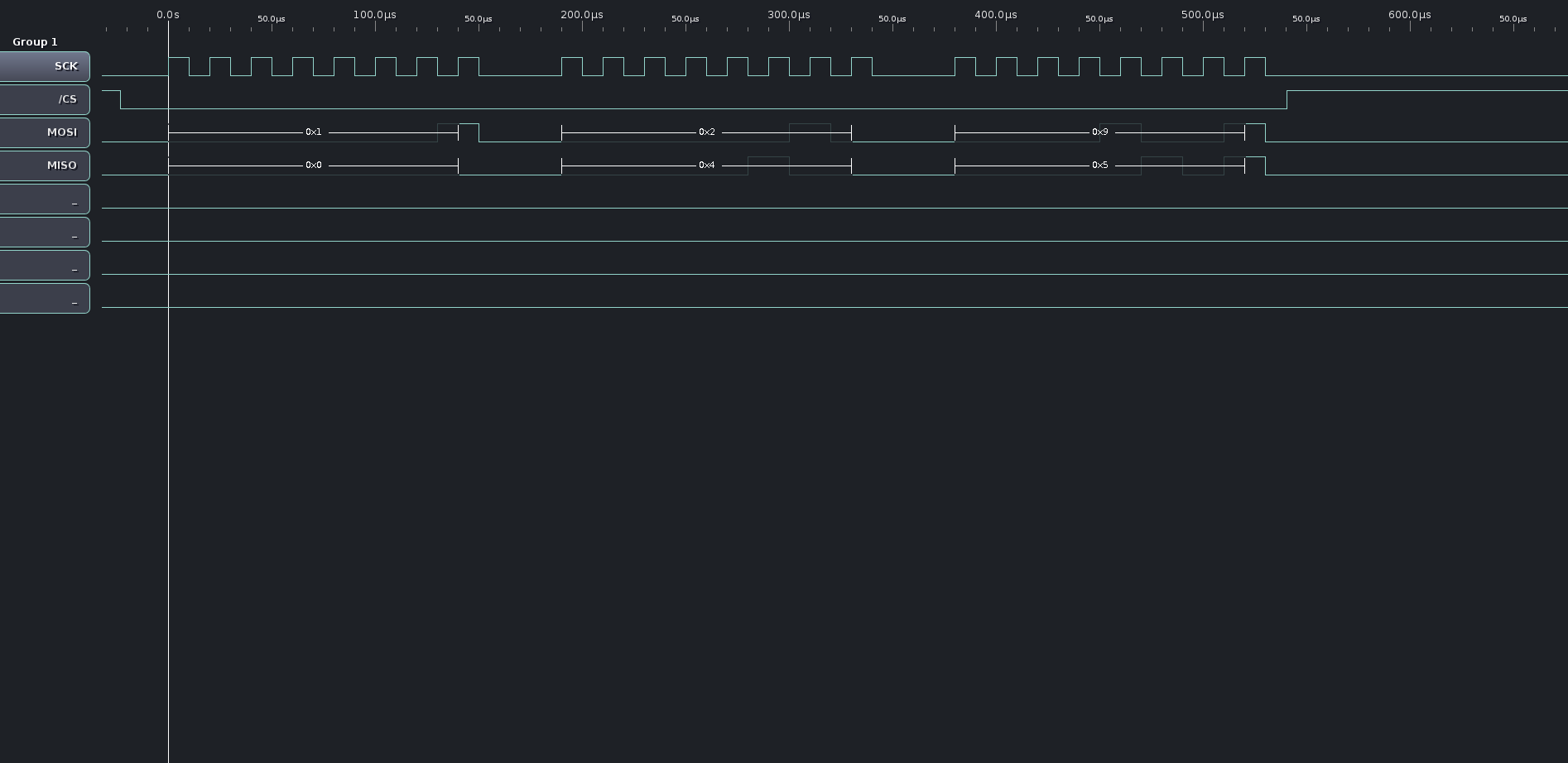
I am using the TIVA TM4C123BH6ZRB and want to send 256*16Bit-data via SSI0 (Master-Mode, Clock=6MHz, DataWidth=16Bit).

Before CS-edge arrives, the Tx-FIFO is filled with valid data (before filling the Tx-FIFO is empty, after filling the Tx-FIFO is full).

But when the Clock begins to run the first 16 bit-data on the bus (via scope) is always NULL. On following transmits all the data is out of allignment...

I tried to fill the FIFO via DMA and also very simple via DataPut  (8x16 Bit), but the result is always the same - first 16 Bit-Value is never transferred,

although it is in the FIFO (first Tx 16Bit-value on bus is always NULL)!

The delay between CS edge and clock-run is > 130 µs!

Could this cause the Problem (timeout)?


Thanks in advance,

Tobi 


  • Hello Tobi,

    The code and waveform would be useful to ascertain what is going on. Can you please share the same?

    Regards
    Amit
  •  Hi Amit,

    thanks for reply.

    This is part of my initialization code. The attached picture shows the transmitted first NULL although the FIFO is full and filled with valid data:


          //Clear the FIFOs
             SysCtlPeripheralReset( spi_x->peripheral );

          //GPIO Init
             ...

          //Peripheral Enable
             SysCtlPeripheralEnable( spi_x->peripherieEnable_ssiX );

          MAP_SSIConfigSetExpClk(
             /*Basis-Adresse*/
             (uint32_t)SSI0_BASE;
             /*clock rate supplied to SSI-Module*/
             (uint32_t) SysCtlClockGet(),
             /*data transfer protocol */
             (uint32_t)SSI_FRF_MOTO_MODE_1,
             /*Mode (zum IMX immer als Slave, Output nicht disabled)*/
             (uint32_t)SSI_MODE_SLAVE,
             /*Bitrate SPI-Clock*/
             (uint32_t) 6000000u,
             /*Laenge Datenpaket: 4..16 Bit
              16 Bit(max. Datenbreite ausnutzen) )*/
             (uint32_t)16u
          );

          // INT enable
             ...

          //SSI enable
             MAP_SSIEnable( (uint32_t)spi_x->spi_base );


       -> Cyclic transfer set:

    void DMA_SPIx_DMA_Kanal_Enable( uint8_t spi_nummer, bool receive ){

         ...

           /*Synchronous Serial Interface Run Mode Clock Gating Control:
            -> SSI Module 0 Run Mode Clock Gating Control
               "Enable and provide a clock to SSI module in Run mode"?*/
          if( (    (HWREG( (uint32_t)SYSCTL_BASE + 0x61Cu ))
                 & ((uint32_t)1u << (uint32_t)spi_x->spi_nummer ) ) == 0u ){
            spi_x->errCounter++;
          }

          if( spi_x->slave_master_mode == (uint32_t)SSI_MODE_SLAVE ){
            /*Tx-FIFO not empty?*/
            if( !(HWREG( (uint32_t)(  spi_x->spi_base
                                    + (uint32_t)SSI_O_SR) ) & 0x1u ) ){
              spi_x->errCounter++;
              /*Tx-FIFO kann nur durch SPI-Reset geleert werden:
                -> Reset ist im SPI_Init() enthalten*/
              /*SPI muss neu initialisiert werden (Slave):*/
                /*War Receive bereits enabled?*/
              uint8_t Rx_war_enabled = (uint8_t)( HWREG( (uint32_t)(spi_x->spi_base
                                               + (uint32_t)SSI_O_DMACTL) ) & 0x1u );
              /*Kanal-Ueberschneidung: keinen Fehler melden*/
              dma_kanalueberschneidung &=
               ( ~( (uint32_t)1u << spi_x->udma_kanalnummer_Rx ) );
              dma_kanalueberschneidung &=
               ( ~( (uint32_t)1u << spi_x->udma_kanalnummer_Tx ) );
              /*SPI komplett resetten und neu initialisieren:*/
              SPIx_Init( spi_x->spi_nummer, false );
              if( Rx_war_enabled ){
                //ToDo: Achtung, Rekursion!
                DMA_SPIx_DMA_Kanal_Enable( spi_x->spi_nummer, SPI_RECEIVE );
              }
            }
            /*TX-FIFO empty?*/
            if( !(HWREG( (uint32_t)(  spi_x->spi_base
                                    + (uint32_t)SSI_O_SR) ) & 0x1u ) ){
              spi_x->errCounter++;
            }
              /*Tx-FIFO mit den ersten Werten fuellen, bevor Uebertragung beginnt:*/

     //-> FIFO is empty
      else{
         for( uint32_t cnt = 0u; cnt < 8u; cnt++ ){
          /*DataPut-Eintraege landen direkt im FIFO (Kein Ring, max. 8x!)*/
            SSIDataPut( spi_x->spi_base, 0xFF00u + (uint32_t)cnt + 1u );
         }

                //-> FIFO is full (SSI_SR_TFE=0, SSI_SR_TNF=0, SSI_SR_BSY=1)

          /*Transfer from Stopp-Mode back to Basic-Mode.*/
          MAP_uDMAChannelTransferSet( spi_x->udma_kanalnummer_Tx
                                      |  (uint32_t)UDMA_PRI_SELECT,
                                      (uint32_t)UDMA_MODE_BASIC,
                                      /*SourceAddr*/
                                      (void *)spi_x->TxBlockdaten_per_DMA,
                                      /*DestAddr*/
                                      (void *)((uint32_t)(  spi_x->spi_base
                                                          + (uint32_t)SSI_O_DR )),
                                      /*Anzahl der Datenbloecke*/
                                      spi_x->blocklaenge_in_16_bit );

           /*start Tx-transmit to via uDMA (fill Tx-FIFO):
          (DMA-Request erfolgt unmittelbar nach Enable
            -> DMA writes 8x16 Bit in the Tx-FIFO):*/
         // uDMAChannelEnable( spi_x->udma_kanalnummer_Tx );

          /*Ist SPI wirklich enabled und uDMA scharf?*/
          if( !( ( ( HWREG( (uint32_t)(spi_x->spi_base + (uint32_t)SSI_O_DMACTL) ) )
                       >> 1 ) & 0x1u    ) ){
            spi_x->errCounter++;
          }

          /*Interrupt fuer "TX FIFO half full or less" vor jeder Uebertragung
            enabeln!
            (uDMA-CompletionInterrupt gilt nicht, da die letzten Tx-Daten zwar im
             FIFO-Puffer, aber noch nicht auf dem Bus sind, wenn CS-Pin
             umkonfiguriert wird!)*/
          //ToDO:
          MAP_SSIIntEnable( spi_x->spi_base, (uint32_t)SSI_TXFF );


              }//end if(Slave Transmit)

    }


  • Hello Tobi,

    Then why is the SSI configured as a Slave device?

    /*Mode (zum IMX immer als Slave, Output nicht disabled)*/
    (uint32_t)SSI_MODE_SLAVE,

    Regards
    Amit
  • Hi Amit,
    the SPI master that communicates with the tiva is an i.MX6 quadCore processor running on Linux.
    The TIVA is SPI slave and has to receive / send data for the exchange via MISO/MOSI.
    Sorry, the Picture is titled incorrect - the red line is unimportant and the blue line Shows the MISO data (data sent from TIVA to i.MX).
    The data that the TIVA receives from the i.MX is handled correctly, but not the Tx data. When the i.MX begins to clock, the first Tx-Transfer from the TIVA is Null!
    I woud be thankful for any kind of idea!
    Regards,
    Tobi
  • Hello Tobi,

    Simplify: Did you try to the same using CPU instead of DMA?

    Regards
    Amit
  • Hi Amit,


    yes, the coding example above runs without DMA. I tried to fill the Tx-FIFO via DataPut():

         for( uint32_t cnt = 0u; cnt < 8u; cnt++ ){
          /*DataPut-Eintraege landen direkt im FIFO (Kein Ring, max. 8x!)*/
            SSIDataPut( spi_x->spi_base, 0xFF00u + (uint32_t)cnt + 1u );//->writes the values to SSIDR Data-Register
         }

    But the result is still the same:-(

    I switched the DMA totally off and fill the FIFO simply by writing values on the SSIDR DataRegister, which are copied into the Tx-FIFO on Register Write.

    So the Slave has to wait until a clock Signal fetches the Tx-FIFO. But the first entry is always transferred as 0...

    Now I'll try to transfer data not to an i.MX processor but to another tiva...

    Regards,

    Tobi

  • Hello Tobi

    I tried the same thing with a SSI Slave and preloading the data into TXFIFO using CPU and it gets transmitted.

    Regards
    Amit
  • Hi Amit,

    thanks for testing your SSI Slave!

    Meanwhile I found the cause why the first sent data was NULL and fixed it. Now it works fine!

    I have to disable the SSI module (clear the SSE bit in the SSICR1 Register) while writing the first 16 bit word into the Tx-FIFO!

    Filling the following FIFO-values can happen with enabled SSI (only the first entry is critical).

    Using the DMA means to write the first entry by Hand while the SSI is disabled and after this the DMA can be enabled

    to to the rest...

       //...
       //SSI_Init() while SSIDisable
       //...
       //SSIEnable()
      
       SSIDisable( (uint32_t)spi_x->spi_base );
       SSIDataPut( spi_x->spi_base, (uint32_t)spi_x->TxBlockdaten_per_DMA[0u] );
          SSIEnable( (uint32_t)spi_x->spi_base );
          /*Set the DMA_TransferSet*/
          MAP_uDMAChannelTransferSet( spi_x->udma_kanalnummer_Tx
                                      |  (uint32_t)UDMA_PRI_SELECT,
                                      (uint32_t)UDMA_MODE_BASIC,
                                      /*SourceAddr -> to 2. Word*/
                                      (void *)(spi_x->TxBlockdaten_per_DMA + 1u),
                                      /*DestAddr*/
                                      (void *)((uint32_t)(  spi_x->spi_base
                                                          + (uint32_t)SSI_O_DR )),
                                      /*Amount of data blocks*/
                                      spi_x->blocklaenge_in_16_bit -1u );


    Regards,

    Tobi

  • Hello Tobi,

    That is not the case on my test. I enabled the Slave and then wrote the first data byte.

    Regards
    Amit
  • I can confirm Tobi's findings. The attached code is a basic test showing the problem: it exchanges 3 bytes between SSI2 (master) and SSI3 (slave) (to be used with the booster pack sockets of an ek-tm4c1294xl). In the form posted everything is fine because SSIEnable(SSI3_BASE); is called within the send for loop after the first slave to master byte was put into the FIFO. However, if you enable SSI3 before the loop (commented out) the first put is ignored and a 0 is transmitted on MISO. I have also confirmed this with a logic analyzer and have attached screenshots of both cases. The TM4C1294NCPDT used is revision 2 AFAIK but I could test this on revision 3 as well if need be.

    #include <stdint.h> /* C99 header for uint*_t types */
    #include <stdbool.h> /* Driverlib headers require stdbool.h to be included first */
    #include <driverlib/gpio.h> /* Supplies GPIO* functions and GPIO_PIN_x */
    #include <driverlib/sysctl.h> /* Supplies SysCtl* functions and SYSCTL_* macros */
    #include <inc/hw_memmap.h> /* Supplies GPIO_PORTx_BASE */
    #include <inc/hw_types.h> /* Supplies HWREG macro */
    #include <driverlib/ssi.h> /* Supplies SSI* */
    #include <driverlib/pin_map.h> /* Supplies mapping of peripherals to pins (for all parts) */
    
    static uint32_t g_sysclk;
    
    #define NUM_SSI_DATA (3)
    
    #define F_SPI (50*1000)
    
    int main (void)
    {
        int i;
        uint32_t buf_master[NUM_SSI_DATA] = {1,2,9};
        uint32_t buf_slave[NUM_SSI_DATA] = {3,4,5};
    
        g_sysclk = SysCtlClockFreqSet((SYSCTL_XTAL_25MHZ |
                                       SYSCTL_OSC_MAIN |
                                       SYSCTL_USE_PLL |
                                       SYSCTL_CFG_VCO_480),
                                      120*1000*1000);
    
        /* SSI Master config (Booster Pack 1) */
        SysCtlPeripheralEnable(SYSCTL_PERIPH_GPIOD);
        SysCtlPeripheralEnable(SYSCTL_PERIPH_SSI2);
    
        GPIOPinConfigure(GPIO_PD3_SSI2CLK);
    //    GPIOPinConfigure(GPIO_PD2_SSI2FSS); // The (only) SS pin of SSI2 is not available on BP1 -> use PN3 instead
        GPIOPinConfigure(GPIO_PD1_SSI2XDAT0);
        GPIOPinConfigure(GPIO_PD0_SSI2XDAT1);
    
        GPIOPinTypeSSI(GPIO_PORTD_BASE, GPIO_PIN_3 | GPIO_PIN_1 | GPIO_PIN_0);
    
        // Alternate CS
        SysCtlPeripheralEnable(SYSCTL_PERIPH_GPION);
        GPIOPinTypeGPIOOutput(GPIO_PORTN_BASE, GPIO_PIN_3);
        GPIOPinWrite(GPIO_PORTN_BASE, GPIO_PIN_3, 0xFF);
    
        SSIConfigSetExpClk(SSI2_BASE,
                           g_sysclk,
                           SSI_FRF_MOTO_MODE_0,
                           SSI_MODE_MASTER,
                           F_SPI,
                           8);
    
        SSIEnable(SSI2_BASE);
        /* Master config done */
    
    
        /* Slave Config (Booster Pack 2) */
        SysCtlPeripheralEnable(SYSCTL_PERIPH_GPIOQ);
        SysCtlPeripheralEnable(SYSCTL_PERIPH_SSI3);
    
        GPIOPinConfigure(GPIO_PQ0_SSI3CLK);
        GPIOPinConfigure(GPIO_PQ1_SSI3FSS);
        GPIOPinConfigure(GPIO_PQ2_SSI3XDAT0);
        GPIOPinConfigure(GPIO_PQ3_SSI3XDAT1);
    
        GPIOPinTypeSSI(GPIO_PORTQ_BASE, GPIO_PIN_0 | GPIO_PIN_1 | GPIO_PIN_2 | GPIO_PIN_3);
    
        SSIConfigSetExpClk(SSI3_BASE,
                           g_sysclk,
                           SSI_FRF_MOTO_MODE_0,
                           SSI_MODE_SLAVE,
                           F_SPI,
                           8);
        /* Slave config done. NB: without SSIEnable! */
    
    //    SSIEnable(SSI3_BASE);
    
        /* Sending 3 bytes with CS pullsed low... */
        GPIOPinWrite(GPIO_PORTN_BASE, GPIO_PIN_3, 0);
        SysCtlDelay(50);
        for(i = 0; i < NUM_SSI_DATA; i++)
        {
                SSIDataPut(SSI3_BASE, buf_slave[i]); // Supply slave -> master data
    
                /* If we enabale SSI3 i.e. the slave before the first FIFO write
                 * 0 will be sent from slave to master in first byte. Why!?
                 */
                if (i == 0)
                    SSIEnable(SSI3_BASE);
    
                SysCtlDelay(50);
                SSIDataPut(SSI2_BASE, buf_master[i]); // Initiate actual transfer
        }
    
        /* Wait till master is done before lifting CS */
        while(SSIBusy(SSI2_BASE))
            ;
        GPIOPinWrite(GPIO_PORTN_BASE, GPIO_PIN_3, 0xFF);
    
        /* Read results from FIFOs */
        for(i = 0; i < NUM_SSI_DATA; i++)
        {
            SSIDataGet(SSI3_BASE, &buf_slave[i]);
            SSIDataGet(SSI2_BASE, &buf_master[i]);
        }
    
        while(1) {
        }
    }


    SSI3 disabled before 1. put:


    SSI3 enabled during 1. put: