This thread has been locked.

If you have a related question, please click the "Ask a related question" button in the top right corner. The newly created question will be automatically linked to this question.

No VDDC is present on my Tm4c1294NCPD Board

 Device on my custom board never connected again to Network, so I checked MAC address with Flash utilities, I set again then I try'd debugging, processor debugger started then at first step reached ISR fault... No way to step, so I measured VCC and is 3.3V VDDC is zero. Oscillator is running (not an xtal a 3.3V 25MHz oscillator.

 VDDC line is not shorted, measuring with a multimeter 4K impedance is present and a 0.5V can be imposed injecting  very small current in the order of few tens uAmp.

 Processor is an Early XM4C1294 got at beginning of 2014. I just own some more early sample (c129ncdp) dated 2013 but I don't risk mount them.

 Is processor to be reworked or can try some trick? Can I supply VDDC core from external? If yes some core low voltages are ready on FPGA too.

 Processor is warm and nothing than debug was done to try isolate network fault.

 I am migrating away from TI processors due to worst policy but this board costed me too much and I need it to finish startup.

  • Bonjourno Roberto,

    Recall that VDDC springs from the MCU core in concert with well chosen & closely located capacitors.   Those caps are (usually) tightly spec'ed - perhaps a cap has gone, "out of range" or there is a routing and/or connection issue.

    I would not try to, "Supply VDDC from an external supply" - only the tightly spec'ed caps should connect.

  • Hi CB1, thank for answer but remember I was one of pioneer on CCS debug and hardware beta test too... I know in deep RF theory math and programming language, so I am not the "Arduino" teacher who is asking about |= &= notation... Just remember Mr Bla Bla Bla Blake pretend me teach for free and use crap. So they "super guru "do a search to catch the work" are not useful. As I marked with like your and Amit recent post, still my old post are of help... I read data sheet and also design guide from early NDA releases.
    Board is a multilayered so VDDC are connected to very close capacitors and line is crossing from pin to pin in min span between two ground layer, inductive path is minimal and HF impedance is low and controlled. Remember I am not the frequentor of this forum nor Blake, I am an electronic engineer qualified experienced and this early board got an year working near perfection.
    About VDDC I am not sure of nothing but I measured voltage on a Launchpad then I used a power supply to impose VDDC, it draw about 13mA, I can read and program flash but processor is stuck. it WAS an XM early sample.
    One other important assurance for industry is missing, see here:
    www.st.com/.../SC1169
    So I encountered too many people hate TI... Thank Mr Blake, your policy of using engineer as free support of kid social network is really great, all perceived this as extremely arrogant, industry and distributor don't like ear about TI and it can drive TI to failure too.
  • Roberto,

    Never was my intent to question your knowledge, skill nor design expertise.    Instead - believing you've been (away) from this space for awhile - and seeking to "echo" that which I've learned from Amit - I answered to the best of my ability.

    From my experience w/other ARM MCUs I've learned that usually - but not always - such core voltages operate similarly to "charge pump" - and as such tightly spec'ed & close proximity caps are required.  

    Should that prove the case here - forcing an external voltage upon VDDC - (well - I'll leave that to you...)

    Really I'd check those caps - and/or measure VDDC to ground (unpowered) just in case small conductive particle has intruded.

    Wish you well - breathe deeply - and "Hi" to monsieur, "Le 4 legged board inspector."   Ciao...

  • cb1_mobile said:
    Never was my intent to question your knowledge, skill nor design expertise.    Instead - believing you've been (away) from this space for awhile - and seeking to "echo" that which I've learned from Amit - I answered to the best of my ability.

     Nor mine but level of answer is far away from details, processor has an LDO and few register relative to it, see late.

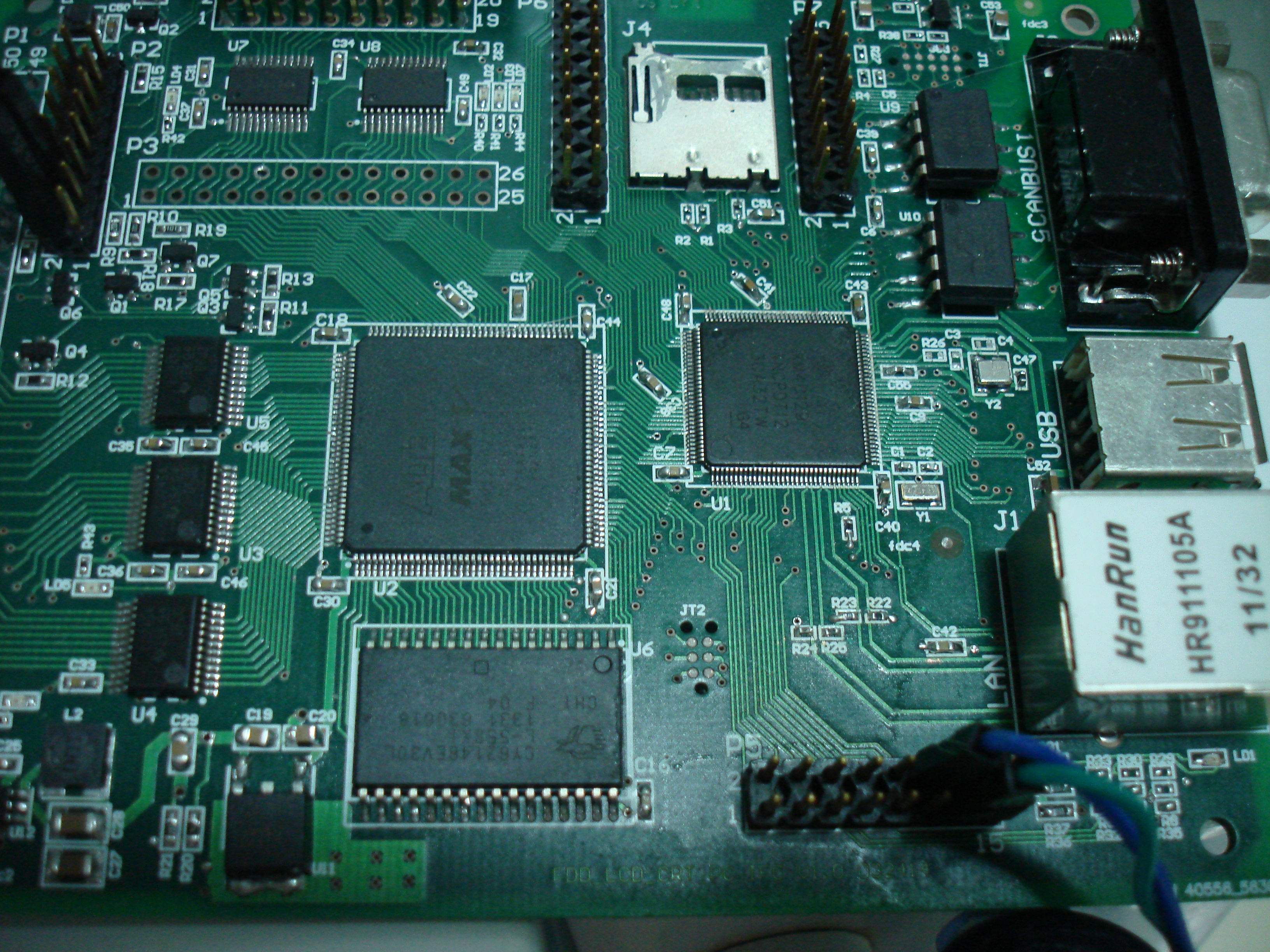
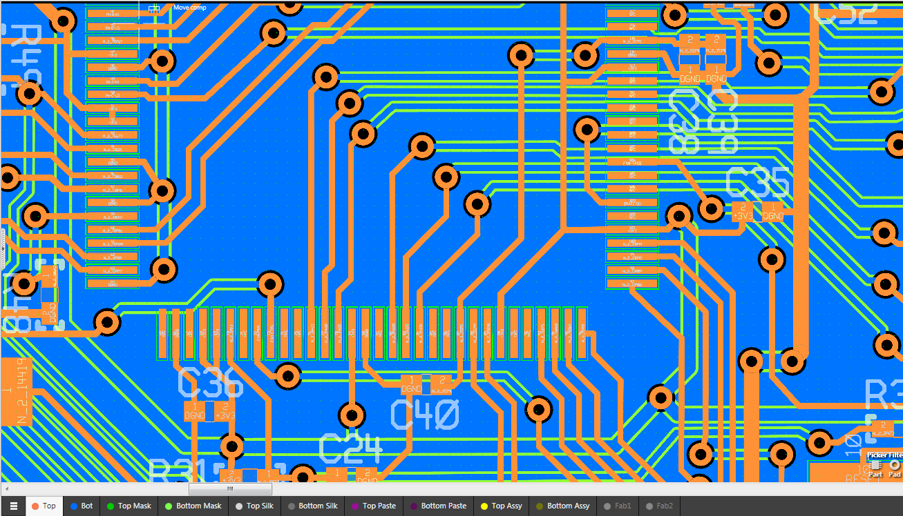
     This is layout, connection is on ground plane and is between the two 3.3V planes, impedance is low and capacitor as you can see are very close to processor.

     To measure capacitance I need remove chip, I feel good to inject DC for resistance measurement but not attach LCR meter so this is reserved after Amit say anything about then I remove faulty device and also measure cap isolation and if you like I can also inject some RF and measure EMF.

     Board is not dirty nor contaminated, it lived just on lab, first demo was at mid of week (this issue I fear it cancel it), enough resolution of picture can show you trace and capacitors. Also read all datecode from MCU.

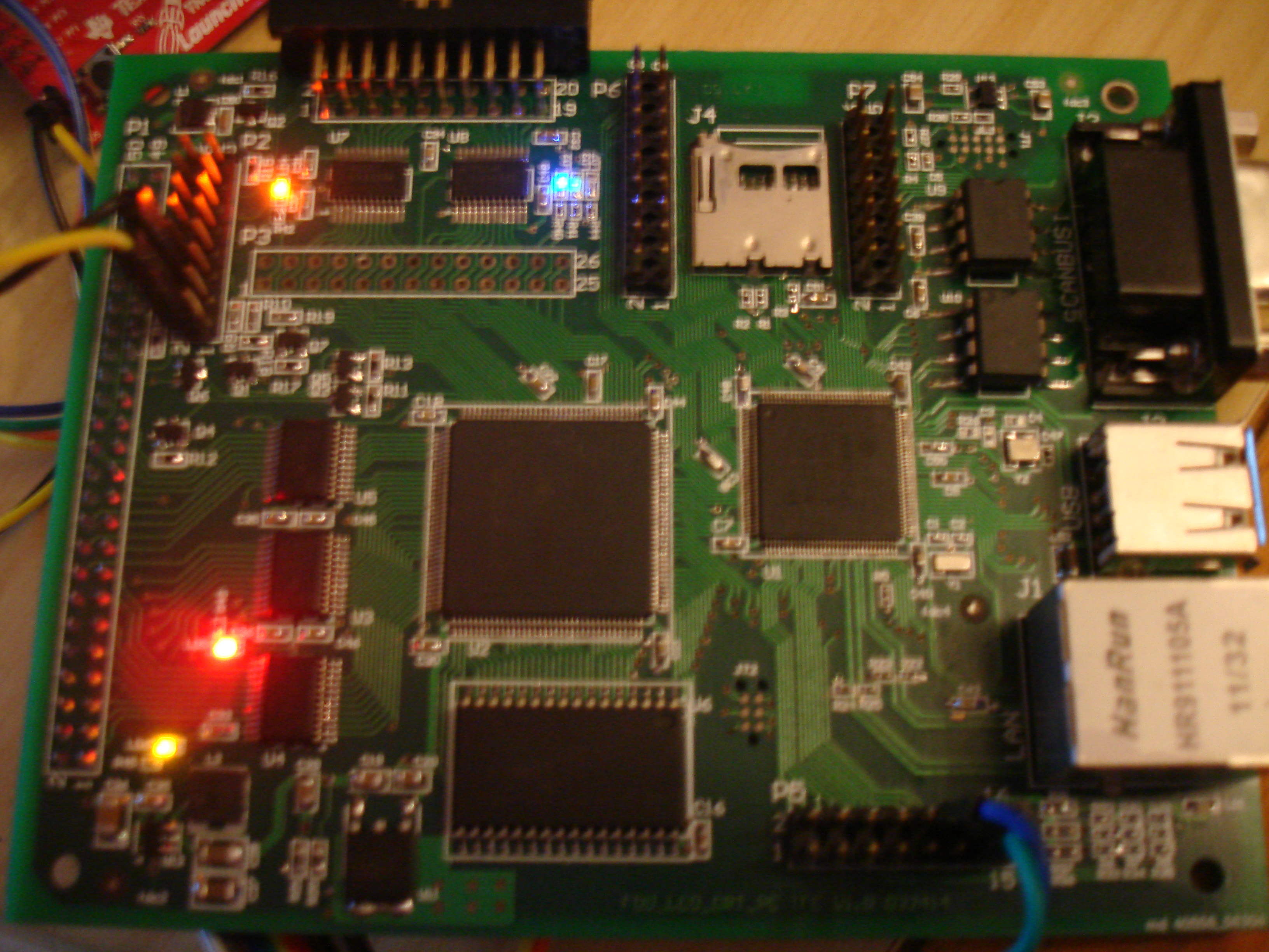
    and here the board powered, power led are all lit, blu and green FPGA activity are on but all MCU LED are off.

    finally the screen of register showing LDO status just after flashing, not sure flashing is really succesful

    About mY inspetcer is not present at moment. I fear he also feel the worst horse we got.

  • cb1_mobile said:
    Really I'd check those caps - and/or measure VDDC to ground (unpowered) just in case small conductive particle has intruded.

    Resistance powereI d or not is forever 4.63KOhm, resistance between capacitor is under 200mOHm I think this is good enough.

     Voltage is 200uV and nothing more is live on MCU.

    Bias resistor (4.87KOhm) measure 4.66KOhm. Both Ethernet strip are terminated over a 100Ohm.

     Oscillator is active and clock internal has no activity sign.

     Tomorrow I take board to lab and I can do some more measure.

  • Terrific detail - thank you.

    I'm no expert w/that family of MCU's - yet the "easiest, least expensive fix" may be the simple exchange of caps w/known good ones. (or - once "out of circuit" your RLC meter may test/verify)

    I'm hoping that Amit will see/advise - but I remain very certain that LDO should not have an external voltage introduced. Again - removal and replacement of LDO connected caps (w/those to "dead-center" of spec) is my suggestion... (while unlikely - cap could have been at the "edge" and may have drifted over time...)

  • cb1- said:
    I'm hoping that Amit will see/advise - but I remain very certain that LDO should not have an external voltage introduced. Again - removal and replacement of LDO connected caps (w/those to "dead-center" of spec) is my suggestion... (while unlikely - cap could have been at the "edge" and may have drifted over time...)

     Hi CB1, I fear you got biased by this forum level, this is not a school project nor hobby one, some hundred of thousand euro where invested on time, this board was designed with certification in mind so no problem to measure capacitor, I connect network analyzer too to see for you how they act over full FCC/CE spectrum.

     So I figured a non invasive method to measure, with a biasing T I insert on DC port  a current limited voltage of about 0.6Vcc, on RF port I attach a signal generator tuned to 50KHz, 50Ohm terminating resistor in series to measuring point so impedance of test fixture is near (50-J0.816)Ohm, an active probe is connected to capacitor, then RF voltage can be easily measured:

     Attenuation of fixture is near -18dB with phase approaching imaginary axis, so when generator is set @ +10dBm probe read -12.3dBm on power meter, from measured attenuation of 22.3dB I infer capacitor exceed 3.9uF by some percent.
     Same test repeated on Spectrum/Network analyzer from 1MHz to 1GHz, attenuation is near expected slope of 10dB/decade (power unit not voltage), phase is near negative imaginary axis so capacitor are out of doubt by I think some order of magnitude.

     I loved really good industry standard MSP430, a resilient processor it work in harsh environment,  I don't like new ARM standard as I never liked at Accorn time.

     So I fear first invasive solution can be only cure the dead horse by replacement, I order from distributor at less than TI sampling policy price, it say I cannot have sample convert to buy @12.5US$, then on basket it cost near 20US$, 3 pcs from Farnell (element14) free shipping cost quite less free of custom fee too...... :(

  • cb1- said:
    I remain very certain that LDO should not have an external voltage introduced.

     There where two regulator family, voltage regulator and LDO, the first generally don't like have voltage at output, if output voltage exceed the input(or set point too) then a SCR like failure is started and regulator get destroyed. LDO generally don't suffer this problem and many of them tolerate regulated port to be supplyed too. If internal LDO is still alive from DC injection seems LDO than voltage topology. Again no data is available from my channel, just who know silicon aka Amit can say what can I measure.
     LM series require a diode from out to in to prevent latchup failure, I never mounted on LDO.

  • Hi,

    My question - did not observed that up to now - do you have a good zero ohm connection between the two VDDC pins? sometimes vias may make subtle problems...

  • Hi Roberto,

    Those suggestions were my best effort - never having used that MCU family - but actively reading/absorbing many posts "touching upon" your issue.

    Sorry if my response was "too basic" - yet I did not find a listing of all of your investigative methods - thus my choice was to "advise" or sit silent.

    Poster Petrei raises a point (via connect) and I'd add that all such pins should be "ohmed out" to confirm.

    Usually - but not always - the presence of extra, identical boards enables (as you know) famed, productive: "A-B-C" testing.    No mention of such board comparison tests and/or results has appeared.    Serious projects are best handled by "multiple builds" (I know this adds expense) and this proves an effective counter to the "schedule slip" you now encounter.

    Good luck my friend...

  • Hello Roberto,

    Great to see you here (though circumstances could have been better). To specifically answer the question LDO must not be supplied externally. The first round of changes would be for the cap checks and if they look fine then change of device. I am not sure why the device would not power up (there is an errata on the X series of 129 devices where LDO may fail to power up) and that was fixed on the TM4C129 production revision.

    Regards
    Amit
  • Hi Amit,

    That's great feedback - and the errata you note appears to well describe Roberto's issue.

    Do you recall if - once LDO fails to power up - that condition remains permanent? (My hope is that - at least for Roberto's testing - multiple power on cycles may restore the LDO voltage - at least upon occasion) This will at least enable (some) testing - far from ideal - but perhaps better than "NOP" no operation.

  • Hello cb1,

    No, the condition is not permanent. On subsequent power cycle it may recover, Why I say may recover, is that in the million+ iterations on the most sensitive of devices we found that two back to back power cycles never failed. It took at least 10+ for the most minimum of power up failures.

    Regards
    Amit
  • Hi Amit,

    Well - Eureka - hope that Roberto sees that! (and glad that I made that connection...)

    Thus - if VDDC's level is monitored w/hi-Z probe (or circuit) Roberto (and/or others) may be able to detect a "successful" power-up!

    At minimum - board testing & code writing may continue until the new/improved device arrives...
  • Hello cb1

    A Rev-3 device with the fix is the correct replacement. However Roberto's experiment on the existing devices with re-power up cycle would show if this is the same issue or is it a complete device failure (due to other conditions unknown right now)

    Regards
    Amit
  • Hi Amit,

    While true - the "risk-reward" for simply trying the, "multiple, repeated power-up tests" seems most worthwhile. Indeed I'd order replacement parts asap (it's truly "urgent" - in this case) yet he's not "ground to a halt" if the MCU can successfully, "power-up."

    In this limited case - (some) operation trumps (no) operation!
  • Amit Ashara said:
    A Rev-3 device with the fix is the correct replacement. However Roberto's experiment on the existing devices with re-power up cycle would show if this is the same issue or is it a complete device failure (due to other conditions unknown right now)

     Hi Amit, are you referring SYSCTL#16? this say

    SYSCTL#16 On-Chip LDO may not Start Properly During Power Up

     My device is forever down, voltage is forever near zero -> 2mV

    I rework device when it arrive, I don't wish build another board as suggested by CB1 so I just try cure this and see what happen.

  • Hello Roberto,

    Yes, that is correct. But if you power cycle the XM4C129 then does it start the second time around?

    Regards
    Amit
  • Amit Ashara said:
    Yes, that is correct. But if you power cycle the XM4C129 then does it start the second time around?

     Hi Amit, this errata was the only one I meet, I interpreted as not working with some voltage present at VDDC and intermittent , my device is forever stuck at 0V never started again, last time was on previous week.

  • Hello Roberto,

    So even on a subsequent power cycle the device remained with a VDDC of 0V? If that is correct, then it must be a damage to the internal regulator. Without a FA it would be not possible to ascertain what happened to the XM4C129 device.

    Regards
    Amit
  • Thank Amit, if you need it I can send but I suppose early experimental devices are of no more interest.
    My wish was an assurance of production plan. Everyone is discouraging me to use TI product so next board, if never done, may be on competitor, this board is for development only so has no sense, when tether get removed this one reach immediate obsolescence, new board is planned on just an FPGA with internal ARM core so I remove both TIVA and OMAP too. This unexpected failure delayed again financial plan and I fear this project still suffer wrong choices of the past.
    See you.
  • Hello Roberto,

    I would suspect so that experimental devices may not be supported for FA (due to the nature of the earlier devices and long list of bug fixes), but normally that would be the route to follow anyhow. I do understand the burn of the devices that you have chosen, but other devices from competitors may also have hidden issues (no to dissuade you from choosing them). At the end of the day it's your choice no matter how much I or any one else rallies.

    Regards
    Amit
  • There is always an increased risk when using parts that are not yet in production (Silicon bugs, supply etc...). I've done it a couple of times, once it was pretty much a disaster and the other quite successful. Both times with large mainstream companies as the source.

    Robert

  • It remains unclear if Roberto has (repeatedly) power cycled his board - which may be the sole means to bring it to operation - while he awaits the new devices. I suspect that this power cycling involves multiple power on/off (say 5x) - perhaps separated by 5 seconds or so.

    Stating that the device is, "forever down" does not clearly convey that multiple, repeated, short duration power cycles have been attempted...
  • Amit Ashara said:
    So even on a subsequent power cycle the device remained with a VDDC of 0V? If that is correct, then it must be a damage to the internal regulator. Without a FA it would be not possible to ascertain what happened to the XM4C129 device.

     Hi Amit, I am back, I finally got new devices on Monday, I mounted on a new board and one other is available to also solder another mcu, I checked all soldering point under microscope, I checked for unsoldered pin, for small short, I quit with new board having the same problem, zero volt on vddc, zero volt on 4k87 resistor for network bias, current drawn from 3.3V rail is very small and processor, fpga too, are cold, oscillators are also unpowered.

     So what can influence vddc and drop to zero? Reading again datasheet I got an Idea but now board is at lab and LP too is there.. so suspence needed and next chapter tomorrow...

  • Hello Roberto,

    This is indeed strange. If the current drawn is in the order of 4-6 mA then it must be RST_n being held low.

    Regards
    Amit
  • Amit Ashara said:
    Hello Roberto,

    This is indeed strange. If the current drawn is in the order of 4-6 mA then it must be RST_n being held low.

    Regards
    Amit

     Hi Amit, time age and worst period I got moved  this board and not only this on stand by. So to have some local status for debugging purpose I decided to add an extra LCD near bard, this required me to use the header expansion port of uC, no free port are on FPGA, I remembered a short was on some unused analog lines and I removed too one more necessary short.

     On design VDDA RLC filter was forgotten so I closed  pin to VDD with a small drop of soldering. I removed it on old board and just checked all solder joint to be clean and connected, from this  I confirm removing VDDA stop LDO, oscillators and network too. Data sheet has some not strong recommendation about VDDA not explaning why is necessary and what are their rule, it just say between lines is necessary also if Analog section get unused.

    Yes I confirm it is MANDATORY otherwise processor get unpowered.

    VDDC capacitor instead require a more close attention to quality and RF impedance due to this line also is linked to PLL, @480Mhz PCB require more caution, so It also need not just to route short, some power plane cut to avoid RF travel on it are to surrounding VDDC track to mitigate RF radiation. On my board radiation is acceptable but my be for two layer board a design tip need be added. So Spectrum analyser stay power down for now and I return to digital domain.

     I am also doing investigative test on unused  hibernation part to see if VBAT can induce some similar strange behaviour to processor. This board s tagged for obsolescence but actually not MAX 10 are available nor final design VHDL code is finished so this board must be reliable to perform his important task on debug and test comparison bridge between old and new hardware in parallel to logic analyser.

     Next week when work is finished I add a note to tip stick thread about common failures

  • Hi Roberto,

    >So what can influence vddc and drop to zero?

    Sounds like you may have answered your own question - flag green?

    >"Leaving the VDDA pin floating stops the internal LDO regulator and results in VDDC measures 0.0V "

    Curious not sure you confirmed in past posts the resistance measured from both VDDC pins to GND when MPU was removed from PCB, please forgive if did so -- missed it along the way here.

    > some power plane cut to avoid RF travel on it are to surrounding VDDC track to mitigate RF radiation. On my board radiation is acceptable but my be for two layer board a design tip need be added.

    Agree asking CB1 recently that very question, not getting a direct confirmation as to pros/cons. How effective is a 2 layer PCB with back side PCB traces wrapped in ground plane to stopping RFI/EMI escaping topside? Does a multilayer center GND plane be more effective this case, or there be trade offs in this area versus cost savings?

    Example: Basically PCB bottom side is the Analog GP that envelopes bottom side traces in AGND. The MPU's DGND/AGND has dedicated trace routes, only a few DGND vector topside by via. All DGND back side PCB similar enveloped in AGND omit .1778mm surrounding air gap each trace. Three buck switchers use AGND, rides slightly below DGND by one EMI/RFI ferrite bead, separates AGND from DGND.

    Didn't like nor trust the LMI approach in the TI-RDK vectoring BLDC motor GND mixed directly into the digital ground plane. Hence the madness to achieve LOW frequency GND isolation on the MOS bridge.
    That isolation of high voltage AGND is a 3.0mm wide trace dedicated mostly to the topside MOS drivers. AGND runs top side PCB into a series (HV-CAP/R) out to FGND screw post. Ensures FGND rides even lower then AGND, that is if anyone elects to run coppers to water pipe or ground rod.
  • So it appears that "floating VDDA" proved the culprit (*) here - both for original MCU and (now) for its replacement.

    Let the record show that even when (and especially when) user does "not plan" to use ANY Analog features of the MCU - VDDA MUST be properly powered & treated.  (emphasis upon "not plan" is due to the fact that (inevitably) at some future point - users "will use" analog!)  

    Let the record show (further) that other ARM MCU vendors have that exact same (power) demand upon VDDA as mentioned here.

    What confounds is "How" the analog section of this MCU was able to perform - if VDDA was improperly terminated and/or powered...   (that should have proved an "easy" catch!)

    (*)  MCU's LDO voltage did not "come up" with the MCU - despite repeated power cycles.

  • cb1_mobile said:
    Let the record show that even when (and especially when) user does "not plan" to use ANY Analog features of the MCU - VDDA MUST be properly powered & treated.  (emphasis upon "not plan" is due to the fact that (inevitably) at some future point - users "will use" analog!)  

     Analog is not planned at all in this board, it is used on slave where 123 part is measuring some voltage and current on board. On one board a slave MSP is present to do a control loop for fast fault action.

     Port incriminated was prepared with idea of differential analog test so you can see from picture top left connector is wired as differential pair.

     Port on this processor also due to usage of EPI are not available and none port is complete 8 bit nor free. This way I prepared LCD driver (Ili1963) to use two half port, one low and one high nibble to minimize software overhead.

     This started the problem I suffered with.

    cb1_mobile said:

    What confounds is "How" the analog section of this MCU was able to perform - if VDDA was improperly terminated and/or powered...   (that should have proved an "easy" catch!)

     I don't know about,  in future may be I can contribute with a comparison.

  • BP101 said:
    Sounds like you may have answered your own question - flag green?

     Hi BP, not for now, I need complete some test then I release this on top stick about common failure about hardware, when I am ready I contact Amit.

    BP101 said:
    Curious not sure you confirmed in past posts the resistance measured from both VDDC pins to GND when MPU was removed from PCB, please forgive if did so -- missed it along the way here.

     I measured both resistance from ground to VDDC and from capacitor to capacitor, I never measured internal resistance from MCU pin alone and I assemble the third board on near future but I don't dismount first prototype nor I plan use other.

    BP101 said:
    Agree asking CB1 recently that very question, not getting a direct confirmation as to pros/cons. How effective is a 2 layer PCB with back side PCB traces wrapped in ground plane to stopping RFI/EMI escaping topside? Does a multilayer center GND plane be more effective this case, or there be trade offs in this area versus cost savings?

     This is not question of cost saving if you are not familiar with RF and current density over a plane. So this is a near single layer than multilayer, you can see it was simple to route VDDC on blu layer but...

     Start layer color and position 1 (Solder) red 2 Ground planes (Brown) 3 Power plane (Cyan) split on left where +5 section is present and 4 soldering side blu.

     VDDC was buried between red and cyan power planes to a path near I supposed it return back to capacitor. This is the less inductive path but remember radiation is another thing. Dont' confuse switching with RF!!! On switch you have to avoid moving application of magnetic field vector, this way is EM so problem come from antennae or radiating planes. A solid plane radiate more than a split slotted one. If you are not familiar with S parameter and RF it is difficult to understand why a plane is worst than a transmission line pair.

    BP101 said:
    Example: Basically PCB bottom side is the Analog GP that envelopes bottom side traces in AGND. The MPU's DGND/AGND has dedicated trace routes, only a few DGND vector topside by via. All DGND back side PCB similar enveloped in AGND omit .1778mm surrounding air gap each trace. Three buck switchers use AGND, rides slightly below DGND by one EMI/RFI ferrite bead, separates AGND from DGND.

     Sorry I cannot understand what this means.

     Air gap? air gap is useless, on motor control no ferrite are on place, Power plane is using one part, then connect to DGND/AGND on one point and AGND is separated by DGND too, power PGND is a big DGND more noisy, one point connection avoid radiating between. Noise on analog tracks is important if you use audio part or need a deep resolution or precision.

    BP101 said:
    Didn't like nor trust the LMI approach in the TI-RDK vectoring BLDC motor GND mixed directly into the digital ground plane. Hence the madness to achieve LOW frequency GND isolation on the MOS bridge.

     Again I cannot understand what this means, also my design has PGND coupled to DGND and AGND, this is the rule but measurement are in some low voltage (Shunt) got differentially, this is suffering less from noise but knowledge has to be grasped.

    BP101 said:
    That isolation of high voltage AGND is a 3.0mm wide trace dedicated mostly to the topside MOS drivers.

     This I think is the right design.

    BP101 said:
    AGND runs top side PCB into a series (HV-CAP/R) out to FGND screw post.

     And also this is a good practice of good design preventing frame ground chassis to discharge ESD nor radiate power EMF.

    BP101 said:
    Ensures FGND rides even lower then AGND, that is if anyone elects to run coppers to water pipe or ground rod.

     I don't know where you live but this is to AVOID, water pipe get corroded by and also it is not assured it is a good earthing point. A good protective earth point MUST be connected to frame ground if metallic and prevention to indirect contact must be applied still if you live in a not civilized country. Life of both human and animals is precious.

  • Hi Roberto,

    This print show 2 layer PCB with integrated GND plane (blue). Cost of same PBC doubles with 4 layer integral GND plane and VDD rail layers.

    Trade off: AGND(blue) encapsulates most all very long runs of MPU signals on bottom PCB. The bright lime green (.1778mm) air gap bottom solder mask. Long ago  a (2 layer integral GND plane) before CAD (auto copper keep out) it was impossible to encapsulate signals in AGND without later having production solder bridges etc... Example of RF perpendicular plus axial vector avoidance technique ,  the top surface signals (orange) have a parallel copper shield (blue) bottom of PCB. That encapsulate most but not all signal paths parallel to the RF radiation plane axis and top surface traces (orange) then have an axial GP below them. That versus the (high cost) perpendicular axial vector RF avoidant multi layer PCB concept.

    Seeming that RF(you mention PLL 480Mhz) tends to escape along the edges of copper traces more than from the center. Perhaps the reason you mention AGND plane is often perforated in ANSI cross hatch. Thanks for reminder, solid versus cross hatching makes a less effective RF sink antenna.  

    Example: Basically PCB bottom side is the Analog GP~~~~

    > Sorry I cannot understand what this means.

  • Hello Roberto,

    The Section on Power Control in System Control Chapter ahs a note that "VDDA must be supplied with a voltage that meets the specification in Table.... or the microcontroller does not function properly..." and then giving further detail that it is required for the clock circuitry

    Regards
    Amit