Other Parts Discussed in Thread: TM4C123GH6PM, EK-TM4C123GXL
Good day,
I am configuring a Tiva Launchpad EK-TM4C123GXL with a Tiva series TM4C123GH6PM with CCSv6. I am programming it to aggregate some analog sensor data, and send it via SPI slave mode to another TI MCU, which is the master. Also, I need to implement some software addressing, because there is another SPI slave on the bus and I can't get a separate chip select.
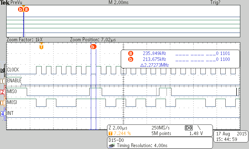
But my immediate issue is the ISR that is configured to be called when the SSI RX FIFO is half full or more. The master is sending out 4 8-bit frames in a row. Since the FIFO is 8 elements deep, every time I get a poll (4 8-bit frames) from the master, it should trip the ISR. In the ISR, I loop through and get all the elements from the FIFO. And before, in the main loop, I have the slave output data already in the TX FIFO. Why is the interrupt only being called every 4 times I poll the slave with the master? Also, the first byte out of 4 is ending up in every element of the recieveData array. The last 3 bytes from the transmit aren't making it through. I have the 4 SPI lines on a scope, and can see the interrupt because I have a GPIO pin toggled high while in the ISR. The master data is correct on the scope. The frame format matches the master, CLK =0 and CPHA = 0.
I attached the main.c file, thanks if you can help explain this.
And right now the data is arbitrary for testing, but soon I am going try and detect the address in the first byte, and if it matches mine, I'll respond, otherwise not. Also, I plan on using:
SSI0_CR1_R &= ~SSI_CR1_SOD //disable the slave output disable
//transmit and other ISR code
SSI0_CR1_R |= SSI_CR1_SOD; //enable the slave output disable

Is this a valid plan of attack? I can't have the slave driving the output line when another slave is transmitting.
/*
* main.c
*/
#include <stdint.h>
#include <stdbool.h>
#include "driverlib/sysctl.h"
//#include "inc/tm4c123gh6pm.h"
#include "driverlib/gpio.h"
#include "driverlib/pin_map.h"
#include "inc/hw_memmap.h"
#include "driverlib/ssi.h"
#include "driverlib/adc.h"
#include "driverlib/interrupt.h"
#include "driverlib/pin_map.h"
#include "driverlib/uart.h"
#include "inc/hw_ints.h"
#include "utils/uartstdio.h"
#include "driverlib/systick.h"
#define SSI0_CR1_R (*((volatile uint32_t *)0x40008004))
#define SSI_CR1_SOD 0x00000008
#define NVIC_ST_CURRENT_R (*((volatile uint32_t *)0xE000E018))
#define NVIC_ST_CTRL_R (*((volatile unsigned long *)0xE000E010))
#define dataLength 4
uint32_t returnData[dataLength] = {0};
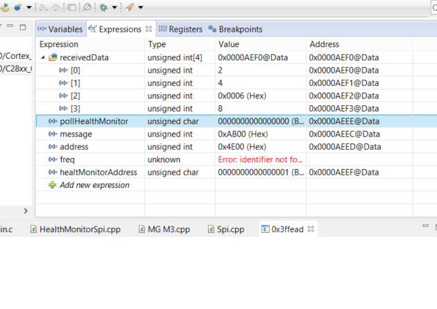
uint32_t receiveData[dataLength] = {0};
uint32_t dataSent = 1;
//returns current system frequency which may not match requested frequency
void Clock_Init(){
uint32_t ui32Config; //provides divisor of one the fixed PLL VCO settings
//PLL is 400MHz: (400MHz/2)/4 = 50MHz
ui32Config = (SYSCTL_SYSDIV_4 | SYSCTL_XTAL_16MHZ | SYSCTL_USE_PLL | SYSCTL_OSC_MAIN);
SysCtlClockSet(ui32Config);
}
void SysTick_Init(){
//15e6/50e6 = 300ms period
SysTickDisable();
SysTickPeriodSet(15000000);
SysTickEnable();
NVIC_ST_CURRENT_R = 0;
}
//configure GPIO to use SSI0 on Port A, SSI1 on Port D
//and AIN0 from slide pot on pin PE3
//Nokia5110 DC
void GPIO_Init(){
//SSI0 is for slave, SSI1 is for LCD
SysCtlPeripheralEnable(SYSCTL_PERIPH_GPIOA); //for slave
SysCtlPeripheralEnable(SYSCTL_PERIPH_GPIOD); //for LCD
SysCtlPeripheralEnable(SYSCTL_PERIPH_GPIOE); //for ADC channels
SysCtlDelay(100);
SysCtlPeripheralEnable(SYSCTL_PERIPH_SSI0);
SysCtlPeripheralEnable(SYSCTL_PERIPH_SSI1);
SysCtlPeripheralEnable(SYSCTL_PERIPH_ADC0);
SysCtlPeripheralEnable(SYSCTL_PERIPH_UART0);
SysCtlDelay(3);
GPIOPinTypeUART(GPIO_PORTA_BASE, GPIO_PIN_0 | GPIO_PIN_1);
//PA2-5:
GPIOPinTypeSSI(GPIO_PORTA_BASE, GPIO_PIN_2 | GPIO_PIN_3 | GPIO_PIN_4 | GPIO_PIN_5);
//PD0-3:
GPIOPinTypeSSI(GPIO_PORTD_BASE, GPIO_PIN_0 | GPIO_PIN_1 | GPIO_PIN_2 | GPIO_PIN_3);
/*
* x axis: PE0 AIN3
* z axis: PE1 AIN2
* offloader force: PE2 AIN1
* temperature: PE3 AIN0
*/
GPIOPinTypeADC(GPIO_PORTE_BASE, GPIO_PIN_0 | GPIO_PIN_1 | GPIO_PIN_2 | GPIO_PIN_3);
GPIOPinTypeGPIOOutput(GPIO_PORTD_BASE, GPIO_PIN_7);//for Data/Command to LCD
GPIOPinTypeGPIOOutput(GPIO_PORTD_BASE, GPIO_PIN_6); //for reset to LCD
GPIOPinTypeGPIOOutput(GPIO_PORTA_BASE, GPIO_PIN_6); //for SSI0 ISR signaling
GPIOPinConfigure(GPIO_PA0_U0RX);
GPIOPinConfigure(GPIO_PA1_U0TX);
GPIOPinConfigure(GPIO_PA2_SSI0CLK);
GPIOPinConfigure(GPIO_PA3_SSI0FSS);
GPIOPinConfigure(GPIO_PA4_SSI0RX);
GPIOPinConfigure(GPIO_PA5_SSI0TX);
GPIOPinConfigure(GPIO_PD0_SSI1CLK);
GPIOPinConfigure(GPIO_PD1_SSI1FSS);
GPIOPinConfigure(GPIO_PD2_SSI1RX);//not used because LCD doesn't transmit back
GPIOPinConfigure(GPIO_PD3_SSI1TX);
}
void UART_Init(){
UARTClockSourceSet(UART0_BASE, UART_CLOCK_PIOSC);
UARTStdioConfig(0, 9600, 16000000);
}
void SSI0_Handler() {
GPIOPinWrite(GPIO_PORTA_BASE, GPIO_PIN_6, GPIO_PIN_6);
//SSI0_CR1_R &= ~SSI_CR1_SOD; //0 in slave output disable bit in order to drive line
SSIIntClear(SSI0_BASE, SSI_RXFF);
//UARTprintf("");
int i = 0;
for(i = 0; i < dataLength; i++){
//wait until a value is in the RX FIFO if there isn't one.
SSIDataGet(SSI0_BASE, &receiveData[i]);
}
for(i = 0; i < dataLength; i++){
UARTprintf("receiveData[%1d] = %08x\n", i, receiveData[i]);
}
dataSent = 1;
UARTprintf("\n");
//disable slave output
//SSI0_CR1_R |= SSI_CR1_SOD;
GPIOPinWrite(GPIO_PORTA_BASE, GPIO_PIN_6, 0x00);
}
//configure and enable the SSI peripheral. Slave mode requires CLK < 12 x system clock (master uC runs SPI at 1.17MHz)
//Using the same polarity and phase as F28M335x: Polarity 0, Phase 1
// means clock idle state is zero, sample takes place on 2nd clock edge
void SSI_Init(){
SSIClockSourceSet(SSI1_BASE, SSI_CLOCK_SYSTEM); //Nokia5110 max f_sclk(ext) is 4.0MHz
SSIConfigSetExpClk(SSI0_BASE, SysCtlClockGet(), SSI_FRF_MOTO_MODE_0, SSI_MODE_SLAVE, 3330000, 8);
//Nokia5110 samples SDIN at positive edge of clock: phase bit should be 1, set idle clock high
SSIConfigSetExpClk(SSI1_BASE, SysCtlClockGet(), SSI_FRF_MOTO_MODE_0, SSI_MODE_MASTER, 3330000, 8);
SSIIntEnable(SSI0_BASE, SSI_RXFF); //SSI0_Handler() will be called when RXFF is half full or more
//For SLAVE
SSIEnable(SSI0_BASE);
//For Nokia5110
SSIEnable(SSI1_BASE);
}
//Configure Interrupts
void NVIC_Init(){
IntEnable(INT_SSI0_TM4C123);
IntPrioritySet(INT_SSI0_TM4C123, 0);
IntMasterEnable();
}
void SysTick_Wait3sec(){
int i;
for (i = 0; i < 10; i++){
while((NVIC_ST_CTRL_R & 0x00010000)==0){
}
}
}
int main(void) {
Clock_Init();
GPIO_Init();
UART_Init();
SSI_Init();
SysTick_Init();
int i;
for (i = 0; i < 4; i++){
returnData[i]=i;
}
NVIC_Init();
while(1){
//get data ready for master initiation
//only put data in return FIFO if the last packet was sent
if (dataSent){
UARTprintf("loading return data\n");
for (i = 0; i < dataLength; i++){
SSIDataPut(SSI0_BASE, returnData[i]);
UARTprintf("returnData[%d]: %08x\n", i, returnData[i]);
}
dataSent = 0;
}
//clear recieveData
for (i = 0; i < dataLength; i++){
receiveData[i] = 0;
}
UARTprintf("Main loop\n");
SysTick_Wait3sec();
}
return 0;
}