This thread has been locked.

If you have a related question, please click the "Ask a related question" button in the top right corner. The newly created question will be automatically linked to this question.

Help Needed with TM4C SPI Read/Write to CC1101

Other Parts Discussed in Thread: CC1101, CC110L

I am attempting to interface a TM4C-1294NCPDT microcontroller with a CC1101 radio using SPI. My launchpad is the EK-TM4C1294XL. My compiler is CCS 6.0.1. The radio board (CC1101EM 3.0) is connected to the board via the EM Adapter BoosterPack such that I have the following connections:

CC1101 Name

TM4C1294 Name

TM4C1294 Port/Pin

Purpose

CSn

GPIO

PP5

Radio control (Hi/Lo)

SCLK

SCLK

PQ0

Clock

SI

SSI3TX/SSI3XDAT0

PQ2/A3

MOSI

SO

SSI3RX/SSI3XDAT1

PQ3/A2

MISO

I used the gpiointerrupt_TivaTM4C1294NCPDT example from the "Getting Started" menu to start with, and added "Board_initSPI();" (which links toEK_TM4C1294XL_initSPI()) to the beginning of my main program.

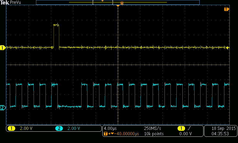
My current task is to write to a single configuration register on the CC1101 (I am using the channel number register), and then read the value back to verify that my writing steps work correctly. Unfortunately the value I read back is always either F0 or 0F, or 1E or E1, or C3 or 3C, or 78 or 87, regardless of what I have written to the configuration register.

This is my reading/writing function:

//Includes
#include "cc1101_functions.h"
#include <inc/hw_memmap.h>
#include <inc/hw_gpio.h>

/* Write to the cc1101 */
uint8 cc1101Write(void)
{

uint32_t pui32DataTx[16];
uint32_t pui32DataRx[16];
uint32_t ui32Index;
uint32_t dummy;

/*All transactions start with a header byte containing a R/W bit, a burst access bit,
and a 6-bit address*/

//Setting addresses, headers, and data to be sent
int address = CC1101_CHANNR; //where in the CC1101 is being written to
uint8_t header_write = (0x00 | address);    //Set up header for writing
uint8_t header_read = (0x80 | address);    //Set up header for reading

//Set up data to be written
pui32DataTx[0]=header_write;

//Data to be written, set up for easy expansion later
for(ui32Index=1; ui32Index<2;ui32Index++)
{
pui32DataTx[ui32Index]= 0x05;
}

//Pull the CSn low
GPIOPinWrite(GPIO_PORTP_BASE|GPIO_O_STATUS,GPIO_PIN_5,0x00);

//Wait until the MISO pin goes low
while (GPIOPinRead(GPIO_PORTQ_BASE|GPIO_O_STATUS, GPIO_PIN_3));

//When not busy, write header for writing data to MOSI Pin
while(SSIBusy(SSI3_BASE)){}                               //Wait for SSI to not be busy
SSIDataPut(SSI3_BASE, pui32DataTx[0]);          //Write header for writing data
SSIDataGet(SSI3_BASE, &dummy);                     //Read dummy values

//When not busy, write data to MOSI Pin
while(SSIBusy(SSI3_BASE)){}                               //Wait for SSI to not be busy
SSIDataPut(SSI3_BASE, pui32DataTx[1]);         //Write data
SSIDataGet(SSI3_BASE, &dummy);                    //Read dummy value

//When not busy, write header for reading data from MISO Pin
while(SSIBusy(SSI3_BASE)){}                             //Wait for SSI to not be busy
SSIDataPut(SSI3_BASE, header_read);            //write header for reading data
SSIDataGet(SSI3_BASE, &dummy);                   //read dummy value

//When not busy, read data from MISO pin
while(SSIBusy(SSI3_BASE)){}                             //wait for SSI to be ready
SSIDataPut(SSI3_BASE, 0x65);                          //Write dummy value
SSIDataGet(SSI3_BASE, &pui32DataRx[0]);    //Read value
pui32DataRx[ui32Index] &= 0x00FF;                  //Mask unnecessary bits

//Pull CSN high
GPIOPinWrite(GPIO_PORTP_BASE|GPIO_O_STATUS,GPIO_PIN_5,0x20);

//Read the chip status byte on the MISO pin
return (GPIOPinRead(GPIO_PORTQ_BASE|GPIO_O_STATUS, GPIO_PIN_3));
}

My main function looks like this:

int main(void)
{
/* Call board init functions */
Board_initGeneral();
Board_initGPIO();
Board_initUART();
Board_initSPI();

cc1101Write();

/* Start BIOS */
BIOS_start();

return (0);
}

And SPI Initialization looks like this:

/*
* ======== EK_TM4C1294XL_initSPI ========
*/
void EK_TM4C1294XL_initSPI(void)
{
SysCtlClockSet(SYSCTL_SYSDIV_10 | SYSCTL_USE_PLL | SYSCTL_OSC_MAIN | SYSCTL_XTAL_25MHZ);

/* SSI3 */
SysCtlPeripheralEnable(SYSCTL_PERIPH_SSI3);

SSIDisable(SSI3_BASE);


// Set IO clock as SSI clock source
//
SSIClockSourceSet(SSI3_BASE, SSI_CLOCK_SYSTEM);

GPIOPinConfigure(GPIO_PQ0_SSI3CLK);
//GPIOPinConfigure(GPIO_PQ1_SSI3FSS); -->This is configured as a GPIO output pin
GPIOPinConfigure(GPIO_PQ2_SSI3XDAT0);
GPIOPinConfigure(GPIO_PQ3_SSI3XDAT1);

GPIOPinTypeSSI(GPIO_PORTQ_BASE, GPIO_PIN_0 | GPIO_PIN_1 |GPIO_PIN_2 | GPIO_PIN_3);

EK_TM4C1294XL_initDMA();
SPI_init();
SSIEnable(SSI3_BASE);
}

  • Hello Matthew.

    When using SSI it is a good idea to monitor the SSI bus as well on a LA/Scope. If you have one available can you please provide a snapshot of the Bus Transaction?

    Regards
    Amit
  • Thank you for your advice. From using the scope we determined that the CSn was not properly being pulled low/high. It did not need a register offset and it has been corrected to: "GPIOPinWrite(GPIO_PORTP_BASE,GPIO_PIN_5,0x20);" to pull high and "GPIOPinWrite(GPIO_PORTP_BASE,GPIO_PIN_5,0x00);" to pull low.

    The following images are from the oscilloscope, taken while the  cc1101Write function was in a continuous loop. The results are representative of what we observed while the program was ongoing. The clock signal (SCLK) is in blue for reference. We observe from these that the CSn is correctly being pulled high and then low again (Figure 1), that the MISO pin is alternating from 0 to 1 every 4 clock ticks (Figure 2), and that the MOSI pin does nothing (Figure 3). We are unsure what to do with this information.

    Figure 1: CSn signal in yellow, clock signal in blue

    Figure 2: MISO signal in yellow, clock signal in blue

    Figure 3: MOSI in yellow, clock signal in blue

  • It is normal in such cases to:

    a) determine that your "dead" MOSI pin is not shorted to ground (or adjacent pin) or is otherwise connected/burdened
    b) after (a) switch that pin into GPIO push-pull output and toggle. Does that yield a measureable output?

    It is possible that your remote device - connected to the MOSI pin of your MCU - is the culprit, too. Also - your ground between that remote IC and the MCU must be solid - and common between each...
  • a) We double-checked that the MOSI pin is not shorted to ground or its adjacent pins with a digital multimeter.
    b) We were unable to get a measurable output using the MOSI or MISO pins as GPIO and toggling manually.

    We checked the ground connections, also using a digital multimeter, they are solid/common for all the boards we have connected together. What does it mean that the remote device may be the culprit? What could we check on the EM to verify correct operation?
  • Hello Matthew,

    If the measurable output of the MOSI in GPIO mode is 3.3V and 0V for logic High and logic Low, then the EM may not be the cause if the EM is still connected. Can you take a register snapshot from CCS when the data transmission is happening, especially the registers for GPIO Port Q?

    Regards
    Amit
  • Matthew Gutierrez said:
    b) We were unable to get a measurable output using the MOSI or MISO pins as GPIO and toggling manually.

    Hi Amit & Matthew,

    Some confusion reigns.   Poster (above, as quoted) states he's, "Unable to achieve output from MOSI or MISO when set to GPIO."   (we assume that set-up is correct as he has gotten output from GPIO config'ed CS.)  

    Next step must be to disconnect any/all connections between the MCU board & external board - and then repeat that MOSI output as GPIO toggle test.

    Unstated (most always) is the "cruel fate" MOSI and/or MISO may have suffered - at any time - prior to this notice.   In our usage of well over 30K ARM MCUs - the number of "DOA" MCU GPIO pins - can be contained on one hand.   (and not all fingers)

    A second MCU board and or slave board should be employed to "escape" the group from "dreaded" Single Board Anomaly...

  • Hello cb1-

    But the poster on the waveform plot shows that the MISO is toggling well between 0V and 3.3V. Then how come it is not measurable?

    Regards
    Amit
  • Amit Ashara said:
    the waveform plot shows that the MISO is toggling

    Indeed it does - yet that "action" is coming from the Slave device - is it not?

    The MCU (aka Master) sits "silent" (w/out output) - and we're not told of its (past) "adventures..."

  • Hello cb1

    Right you are. It would be a good idea to disconnect the CC110L from the EM adapter to isolate the SSI for any monitoring

    Regards
    Amit
  • After looking over the code, there was a mistake in implementing the MISO/MOSI as GPIOs. I was able to output on each pin when they were configured as GPIO. I started with just the MCU board, then added the booster pack, then CC1101, each time getting the same result. So both pins are working as GPIO, so I figure it must be something wrong with my SSI code.

    Thanks again.
  • Hello Matthew,

    Check if the MOSI and MISO pin definition on the two devices is correct.

    Regards
    Amit
  • With luck - this may resolve: from your neat chart (opening post) "SSI3TX/SSI3XDAT0"

    In the SSI init you chose SSI3XDAT0 - I believe SSI3TX (instead) was required for MOSI!

    The "SSI3XDAT0" to my mind - is reserved for "multi-bit" SPI devices - which your CC1101 (clearly) is not...

    And - if that proves correct - you must "kill" the similar (mishandling) of MISO.

  • Our SSI initialization was the problem. We needed to use the SSIConfigSetExpClk function to fully initialize the SSI. Here is the working initialization code:

    /* SSI2 */
    SysCtlPeripheralPowerOn(SYSCTL_PERIPH_SSI2);
    SysCtlPeripheralEnable(SYSCTL_PERIPH_SSI2);
    SSIDisable(SSI2_BASE);

    // Set IO clock as SSI clock source
    SSIClockSourceSet(SSI2_BASE, SSI_CLOCK_SYSTEM);

    GPIOPinConfigure(GPIO_PD3_SSI2CLK);
    //GPIOPinConfigure(GPIO_PD2_SSI2FSS);
    GPIOPinConfigure(GPIO_PD1_SSI2XDAT0);
    GPIOPinConfigure(GPIO_PD0_SSI2XDAT1);

    SSIConfigSetExpClk(SSI2_BASE,SysCtlClockGet(),SSI_FRF_MOTO_MODE_0,SSI_MODE_MASTER,32000,8);

    GPIOPinTypeSSI(GPIO_PORTD_BASE, GPIO_PIN_0 | GPIO_PIN_1 | GPIO_PIN_2 | GPIO_PIN_3);

    //EK_TM4C1294XL_initDMA();
    //

    SSIEnable(SSI2_BASE);
    SPI_init();
    }

    Thanks for all the help.