This thread has been locked.

If you have a related question, please click the "Ask a related question" button in the top right corner. The newly created question will be automatically linked to this question.

How to use SPI in TM4C123G without a frame synchronization?

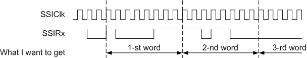
I strongly need to use SPI with DMA in the receiving mode without the frame synchronization. I tried to use Motorola modes (when SPI becomes active if you set 0 on the FSS pin) but I've got a fail. Regardless of which level which I set on the FSS pin SPI doesn't want to receive an information. It seems like receipt is possible only by the edge of the FSS signal not on the constant level on it. Is it true? Is it possible to receive without FSS at all?

  • Hello Tankist,

    Code please! and if the SPI is in master or slave mode. Note that the some of the SPI pins are on Locked GPIO's and would need to be unlocked before they are configured.

    Regards
    Amit
  • I think my source code doesn't matter because it works fine, but if you wish I will publish it.

    #include <string.h>
    #include <stdint.h>
    #include <stdbool.h>
    #include "inc/hw_ints.h"
    #include "inc/hw_memmap.h"
    #include "inc/hw_types.h"
    #include "inc/hw_ssi.h"
    #include "driverlib/gpio.h"
    #include "driverlib/ssi.h"
    #include "driverlib/interrupt.h"
    #include "driverlib/pin_map.h"
    #include "driverlib/sysctl.h"
    #include "driverlib/udma.h"
    #include "system.h"
    #include "dma.h"
    #include "spi.h"
    #include "rtos.h"
    
    #pragma data_alignment=1024
    T_DMA_CHANS ucControlTable[2][32];
    
    uint8_t spi_in_buf[2][SPI_BUF_SIZE];
    
    void dma_init()
    {
    	SysCtlPeripheralEnable(SYSCTL_PERIPH_UDMA);
        uDMAEnable();
        uDMAControlBaseSet(ucControlTable);
    
    	spi0_dma_init();
    }
    
    void SSI0_Handler(void)
    {
    	uint32_t ui32Status;
        uint32_t ui32Mode[2];
    	extern void putToQueTask2ISR(uint32_t val);
    
        ui32Status = SSIIntStatus(SSI0_BASE, 1);
    
    	SSIIntClear(SSI0_BASE, ui32Status);
    
        ui32Mode[0] = uDMAChannelModeGet(UDMA_CHANNEL_SSI0RX | UDMA_PRI_SELECT);
    	ui32Mode[1] = uDMAChannelModeGet(UDMA_CHANNEL_SSI0RX | UDMA_ALT_SELECT);
        
    	if(ui32Mode[0] == UDMA_MODE_STOP)
        {
    		uDMAChannelTransferSet(UDMA_CHANNEL_SSI0RX | UDMA_PRI_SELECT,
            UDMA_MODE_PINGPONG,
            (void*)(SSI0_BASE + SSI_O_DR),
            (void*)spi_in_buf[0],
            SPI_BUF_SIZE);
            uDMAChannelEnable(UDMA_CHANNEL_SSI0RX | UDMA_PRI_SELECT);
    		putToQueTask2ISR((uint32_t)spi_in_buf[0]);
        }
        
        if(ui32Mode[1] == UDMA_MODE_STOP)
        {
    		uDMAChannelTransferSet(UDMA_CHANNEL_SSI0RX | UDMA_ALT_SELECT,
            UDMA_MODE_PINGPONG,
            (void*)(SSI0_BASE + SSI_O_DR),
            (void*)spi_in_buf[1],
            SPI_BUF_SIZE);
            uDMAChannelEnable(UDMA_CHANNEL_SSI0RX | UDMA_ALT_SELECT);
    		putToQueTask2ISR((uint32_t)spi_in_buf[1]);
        }
    }
    
    void spi0_dma_init(void)
    {
        unsigned long delay;
    	
    	memset(spi_in_buf, 0, sizeof(spi_out_buf));
        
        SysCtlPeripheralEnable(SYSCTL_PERIPH_SSI0);
    	SysCtlPeripheralEnable(SYSCTL_PERIPH_GPIOA);
        
        GPIOPinConfigure(GPIO_PA2_SSI0CLK);
    	GPIOPinConfigure(GPIO_PA3_SSI0FSS);
        GPIOPinConfigure(GPIO_PA4_SSI0RX);
        GPIOPinTypeSSI(GPIO_PORTA_BASE,
            GPIO_PIN_2 | GPIO_PIN_3 | GPIO_PIN_4);
        
        for(delay=0; delay<10000; delay++);
    
    	SSIConfigSetExpClk(
            SSI0_BASE,
            80000000UL,
            SSI_FRF_TI,//SSI_FRF_NMW,//SSI_FRF_MOTO_MODE_0,
            SSI_MODE_SLAVE,
            4800,
            8);
       
        uDMAChannelDisable(UDMA_CHANNEL_SSI0RX);
     	uDMAChannelAssign(UDMA_CH10_SSI0RX);
    	
    	// Init DMA-channel for SPI-RX
        uDMAChannelAttributeEnable(
            UDMA_CHANNEL_SSI0RX,
            UDMA_ATTR_ALTSELECT);
        uDMAChannelAttributeDisable(
            UDMA_CHANNEL_SSI0RX,
            UDMA_ATTR_USEBURST | UDMA_ATTR_HIGH_PRIORITY | UDMA_ATTR_REQMASK);
    	
        uDMAChannelControlSet(UDMA_CHANNEL_SSI0RX | UDMA_PRI_SELECT,
            UDMA_SIZE_8 | UDMA_SRC_INC_NONE | UDMA_DST_INC_8 | UDMA_ARB_1);
    	uDMAChannelControlSet(UDMA_CHANNEL_SSI0RX | UDMA_ALT_SELECT,
            UDMA_SIZE_8 | UDMA_SRC_INC_NONE | UDMA_DST_INC_8 | UDMA_ARB_1);
        uDMAChannelTransferSet(UDMA_CHANNEL_SSI0RX | UDMA_PRI_SELECT,
            UDMA_MODE_PINGPONG,
            (void*)(SSI0_BASE + SSI_O_DR),
            (void*)spi_in_buf[0],
            SPI_BUF_SIZE);
    	uDMAChannelTransferSet(UDMA_CHANNEL_SSI0RX | UDMA_ALT_SELECT,
            UDMA_MODE_PINGPONG,
            (void*)(SSI0_BASE + SSI_O_DR),
            (void*)spi_in_buf[1],
            SPI_BUF_SIZE);
    
    	uDMAChannelEnable(UDMA_CHANNEL_SSI0RX | UDMA_PRI_SELECT);
    	
    	SSIDMAEnable(SSI0_BASE, SSI_DMA_RX);
    	SSIEnable(SSI0_BASE);
    	
    	SSIIntClear(SSI0_BASE, SSI_RXFF);
    	SSIIntEnable(SSI0_BASE, SSI_RXFF);
    	IntEnable(INT_SSI0);
    }
    

    I think the main problem is ability of hardware perform that operation. The SPI port works as slave so it can't produce clocks and frame synchronization (receiving SSI has 2 pins only: SSLCLK and SSIRX). Is it possible to receive a signal without the frame synchronization?

    In order to describe the problem I publish a drawing:

    The position the edge of the frame doesn't matter.

  • Hello Tankist,

    On the TM4C12x implementation the FSS or CS pin is required and at least that is what I understand from most of the implementations that a CS is required when connecting in a multi slave environment,

    Regards
    Amit
  • Pardon - but does not your (own) drawing (strongly) support the NEED for the FSS/CS pulse?

    Minus FSS/CS - how does the process ever (effectively) start or end?   (your drawing shows SSIRx activity prior to "1st word.")

    It may well be that the MCU's internal logic paths require the FSS signal to become fully enabled.   (that's the case w/in "other" ARM MCUs)

    FSS potentially (likely) allows the SSI module to be selectively "enabled."   If "on/enabled" forever - it's extremely vulnerable to noise bursts/impulses - is it not?

  • It's easily to understand if you recall a situation when the microcontroller works with an audio codec - the data stream from the codec is infinite, but you don't get any negative situation.

    I can recognize the start of the frame by my own DSP algorithm so I don't need any external signal for that.

    Since it's impossible to use SSI in a slave mode without FSS I will make an external hardware for that. It will be a counter and a few logic elements to provide an artificial FSS signal to the SSI port.

  • @Tankist,

    Believe you've raised good points - and perhaps that enables a simple solution.

    Cannot you create an "artificial" FSS which would result from a "dummy" SSI_Clk pulse's (rising edge) setting an external flip-flop. (Rising edge chosen as you "clock in" your data on the falling edge of SSI_Clk - revealed by your timing chart.   Toggling FSS in this manner (either high or low) provides sufficient set-up time for the SSI module)   We assume that the µDMA prevents your use of a GPIO pin to toggle FSS.   The intent here is to replace that GPIO toggle w/your "normal" SSI_Clk signal in conjunction w/an external flip-flop.

    SSI data - subsequently input into the MCU - is then managed via the MCU's Slave SSI/µDMA modules.   At the completion of the transaction you would "clear" the "FSS flip-flop." 
     
    Cost is one flip-flop - which then allows you to achieve your desired MCU, SSI-µDMA operation - just as you originally sought...

  • Sorry, I don't exactly understand your idea. Could you draw a schematic diagram?
    Generally, the idea of an external synchronization is based on the following principles:
    1) FSS signal must be synchronized with the clock signal (jitter must be as small as it possible).
    2) FSS signal must occur once per 8 bit.
    3) I can't receive any additional signals over a communication link except clocks and data.

  • Before launching into a schematic - my suggestion rested upon your being able to emit a "dummy" SPI_Clk (up-down) - that serving to "create" an artificial "FSS" toggle. After that one dummy SPI_Clk period - "real" SPI clock & data would arrive.

    As "additional signals" are disallowed by your commo link - this flip-flop controlled toggle must (now) be timer-based - the timer serving to "auto-extinguish" FSS upon time-out.

    This method does "not" sync FSS with any valid SPI_Clk - one SPI_Clk is expended to clock the flip-flop which creates FSS.
  • Ok, now I understand. Unfortunately it's impossible to form my own signal through the CLK pin - the clock signal is infinite and I cann't control it.
  • Yes - appears we now both understand the complications & limitations of the MCU w/in your rather unique situation.

    Purely a guess - but if you employed that "flip-flop" suggestion - and if you could some way/how (briefly) "gate off" your clock signal - that "loss of clock" could be detected - and that in turn could enable FSS at the MCU. (we've done similarly upon a navy ship - where communication channels were limited - and we had to "massage out" various control bits...)

    Should your situation be standard - it may pay to see how the "biggies" manage - and see what can be "borrowed (or worse)."