This thread has been locked.

If you have a related question, please click the "Ask a related question" button in the top right corner. The newly created question will be automatically linked to this question.

TM4C123GE6PMI ADC crosstalk issue

Hello,


I have a product based on the TM4C123GE6PMI and I'm having crosstalk between ADC channels.  My setup/configuration:

ADC0 Initial configuration:

    //
	// Initially configure ADC0
    //
    SysCtlADCSpeedSet(SYSCTL_ADCSPEED_500KSPS);
    SysCtlPeripheralEnable(SYSCTL_PERIPH_GPIOD);
	SysCtlPeripheralEnable(SYSCTL_PERIPH_ADC0);		// Enable ADC0 peripheral
	// Set GPIO PE3 as an ADC input
	GPIOPinTypeADC(GPIO_PORTE_BASE, GPIO_PIN_0 | GPIO_PIN_1 | GPIO_PIN_2 | GPIO_PIN_3);
	GPIOPinTypeADC(GPIO_PORTD_BASE, GPIO_PIN_0 | GPIO_PIN_1 | GPIO_PIN_2 | GPIO_PIN_3);

ADC0 Mode configuration:

	ADCSequenceConfigure(ADC0_BASE, 0, ADC_TRIGGER_ALWAYS, 0);
	// Configure over sampling
	ADCHardwareOversampleConfigure(ADC0_BASE, OverSample);
	// Configure Sequencer 0 to sample 4 channels each store in a step
	// Interrupt on step3 -> final step
	ADCSequenceDisable(ADC0_BASE, 0);
	ADCSequenceStepConfigure(ADC0_BASE, 0, 0, ADC_CTL_CH0);
	ADCSequenceStepConfigure(ADC0_BASE, 0, 1, ADC_CTL_CH1);
	ADCSequenceStepConfigure(ADC0_BASE, 0, 2, ADC_CTL_CH2);
	ADCSequenceStepConfigure(ADC0_BASE, 0, 3, ADC_CTL_CH3 | ADC_CTL_IE | ADC_CTL_END);
	// Register interrupt handler
	ADCIntRegister(ADC0_BASE, 0, ADC0IntHandler4ch_TestMode);
	// Clear interrupt flag
	ADCIntClear(ADC0_BASE, 0);
	// Enable interrupts
	ADCIntEnable(ADC0_BASE, 0);

So the Tiva part gets triggered and kicks off the ADC with this configuration pre-loaded.  At power up the Initial configuration is run.  After that and some other system configuring (GPIO, USB etc..) the mode configuration is run.  This is run separately because the speed and number of channels are configured based on parameters stored in EEPROM.  So the params might say run 1 channel at 500k or 4 channels at 1k etc... 

The ADC0 is always configured to run at 500ksps per the

SysCtlADCSpeedSet(SYSCTL_ADCSPEED_500KSPS);

instruction.  So if I want to run 4 channels I effectively get 125ksps/channel.  The problem I'm seeing  with is when I run 4 channels. 


So, to recap the above configuration is what I'm using in this exact situation recording 4 channels with ADC0 speed set to 500k. 
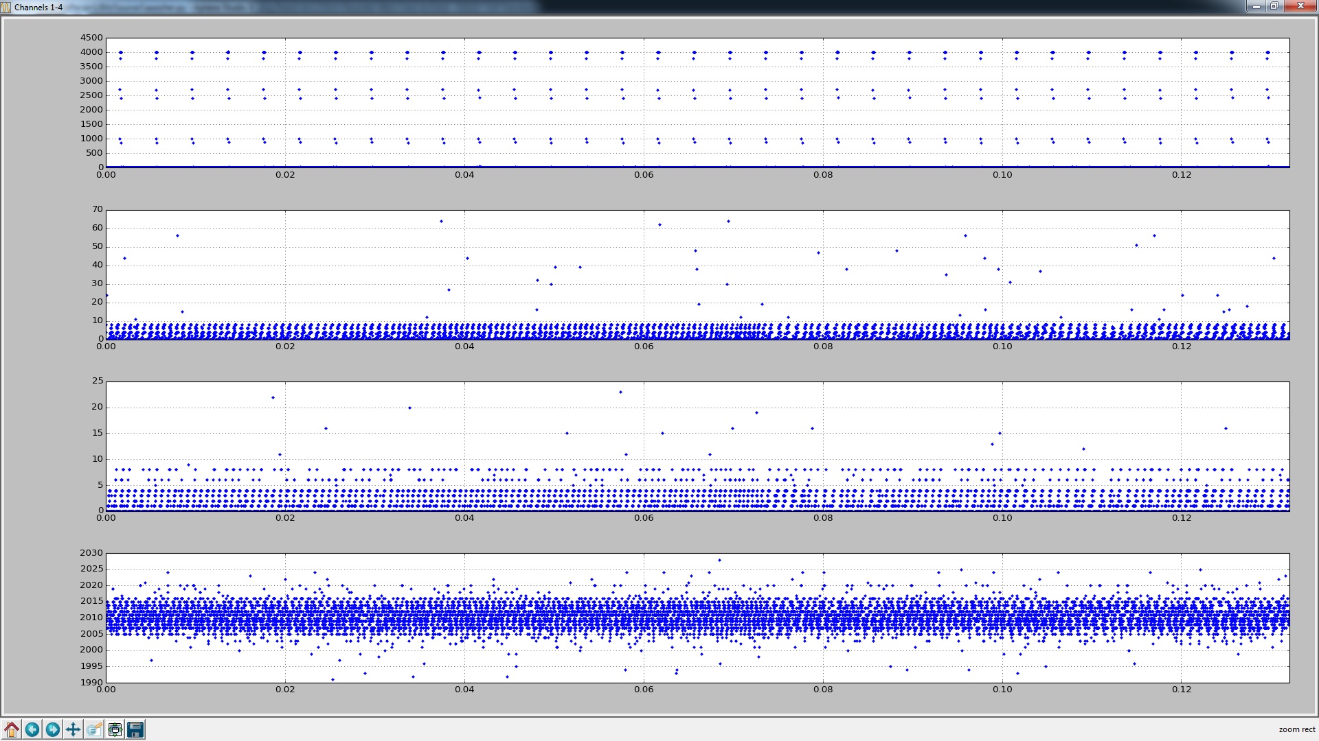
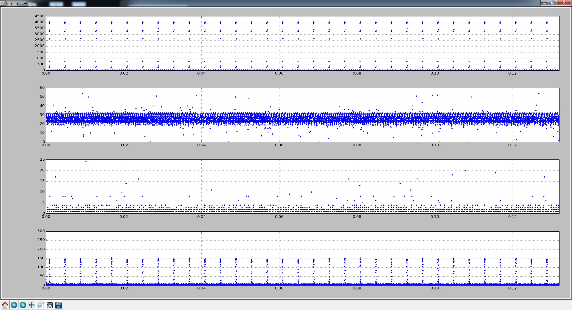
The problem I'm having is this:  If I put a PWM signal into channel 4 and run with the ADC0 configured as above, I get a little bit of the signal in channel 4 bleeding over to channel 1.  So in other words If I run a 3.3V pwm signal into channel 4 with channels 2 and 3 grounded I see the below plot...

Channel 1 really should be around 0v (roughly) like channels 2 and 3.  Some how channel 4's signal is  getting into channel 1.  I thought I would be pretty safe running this at 500k since it isn't the max speed.  I would have though the adc cap could discharge pretty easily by then.  I'm not sure exactly what is going on.  The input of channel 1 has an op amp driving it, but the op amp is AC coupled.  Shown below:

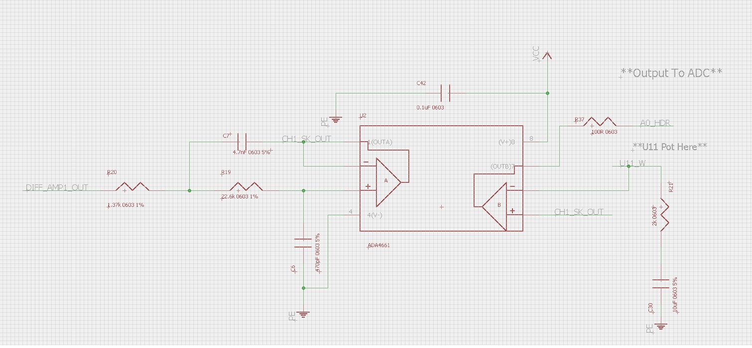
The PWM signal comes in through R20 (Sallen key LPF) and then into a gain stage.  Between A0_HDR and U11_W nets is a digital POT which allows me to adjust the gain via I2C.  The 100R is inline with the output as recommended by analog devices for stability.  So yes, the 100R is IN SERIES with the ADC0 Channel1 that is experiencing this problem. 


I don't see this problem when I put a scope probe at the input of channel1 and let the pwm signal run continuously through this analog circuit.  I ONLY see this pulses on ch1 when I sample the four pins with the ADC.  I'm not sure if this is a ADC configuration problem or a problem with the way I'm driving the channels, but I'm out of ideas troubleshooting and am looking for some new fresh perspectives/ideas. 


If anyone has any insight it would be helpful. 

As a note for what circuits are driving what channels (ch1 -> ch4) the above op amp circuit is driving channels 1 and 2.  The below circuit is driving channels 3 and 4.  I DO NOT see this problem on channel 3 when the ADC channel 3 pin is ungrounded and left being driven by the below circuit so I'm leaning towards this possibly being an issue because ch1 and ch2 opamp circuits are ac coupled and don't drive a "DC" signal into the pins as the below circuit for ch3 and ch4 do.

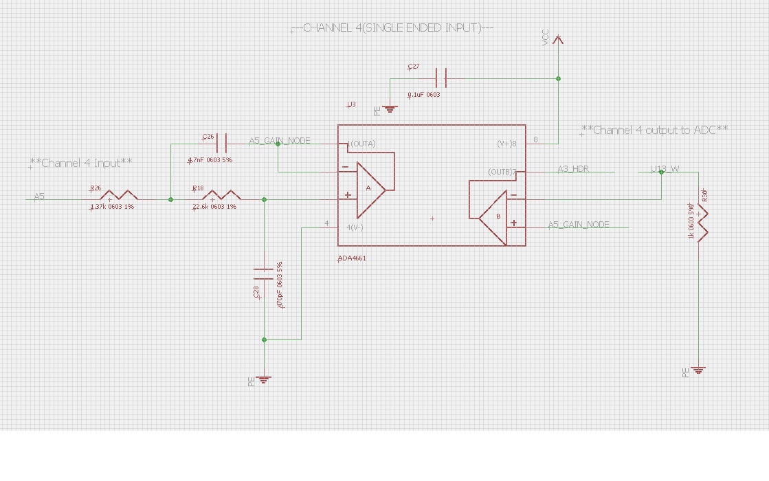
The break between nets A3_HDR and U13_W is where the digital POT goes allowing me to adjust gain here just like above.  The big difference is the AC coupled part but I don't understand how this could produce this problem.

Thanks,

Rob

  • Also forgot to mention. When I run in this manner but instead of constant sampling I trigger more slowly off of a timer this problem goes away. I leave the adc configured to run at 500ksps, but I use a timer to trigger the adc to sample say 50ksps so the timer kicks off the adc 50k times per second I don't see this issue. It seems to be that I'm running at 500k per 4 channels in the constant sampling mode.
  • Feel your pain.    Following may assist:

    • there is an errata issue w/the ADC - do check (may/may not describe your issue)
    • friend Robert here has advocated for low value bypass cap placed closely to the MCU's ADC pin(s)

    Many have noted this apparent "crosstalk/bleeding" across multiple MCUs (not just this vendor).   Real (pro) ADCs go thru pains to better isolate signal paths - guard against such.   Mixed signal devices - not having that luxury - are susceptible.

    Often - this effect varies between different channels.   (not much help if your board is complete - but may improve next rev...)

  • Hello cb1

    I do see the errata taking affect here where the channel 4 is bleeding into channel 1.

    Robbie,

    Instead of sampling 1-2-3-4, if the order is changed to 4-3-2-1 do you still see the issue?

    Regards
    Amit
  • Hi amit and cb1,

    Thank you for the response!  I'm using the sequencer with this part.  The ADC has a single byte, 4 byte and 8 byte sequencer and I'm using the 8 byte one.  I run 4 bytes deep and interrupted.  From what I remember you setup what input channel to start atband it runs through them in order until it hits the channel that generates an interrupt.  I didn't know you could reverSe the channel order.  Are you sure this is possible?

  • Hello Robbie,

    The Channel Mapper is fully programmable. That means if you want one channel to be sampled more often then in a 8 step sequencer it is possible to do the following

    ChA-ChB-ChA-ChC-ChA-ChD-ChA-ChE

    such that ChA is sampled 4 times and ChB, ChC, ChD and ChE are sampled once. This can be reordered as

    ChA-ChA-ChA-ChA-ChB-ChC-ChD-ChE

    Regards
    Amit
  • cb1- said:
    friend Robert here has advocated for low value bypass cap placed closely to the MCU's ADC pin(s)

    Absolutely. As does TI (and other suppliers) in their application notes.

    If I understand what's drawn there does not appear to be an input cap on the A/Ds rather the input is driven directly by the op-amps. You would need on the order of 100Mhz or better response from the op-amp in that scenario,

    Robert

  • Robert you are correct. There are NO input caps on the ADC. The ADC inputs are tied directly to the output of the op amps. Is this a problem? Are you and cb1 recommending input caps on the ADC? I'm just looking for a little clarity as I'm a bit unsure. Also robert could you elaborate briefly on the op amp requiring a 100mhz response? It sounds like this 100mhz response is required if I add input caps. I may be completely misunderstanding this so I'm just looking for some clarification.

    Amit - I will work on switching up the channels tonight to see of that helps. Is the information regarding how to configure the sequencer in the data sheet? I don't recall seeing that in the past. At least not in the tiva 123 data sheet.

    Thanks guys!
  • Hello Robbie,

    It is in the manner you assign each step of the ADC sequencer

    ADCSequenceStepConfigure(ADC0_BASE, 0, 0, ADC_CTL_CH0);
    ADCSequenceStepConfigure(ADC0_BASE, 0, 1, ADC_CTL_CH1);
    ADCSequenceStepConfigure(ADC0_BASE, 0, 2, ADC_CTL_CH2);
    ADCSequenceStepConfigure(ADC0_BASE, 0, 3, ADC_CTL_CH3 | ADC_CTL_IE | ADC_CTL_END);

    would change to

    ADCSequenceStepConfigure(ADC0_BASE, 0, 0, ADC_CTL_CH3);
    ADCSequenceStepConfigure(ADC0_BASE, 0, 1, ADC_CTL_CH2);
    ADCSequenceStepConfigure(ADC0_BASE, 0, 2, ADC_CTL_CH1);
    ADCSequenceStepConfigure(ADC0_BASE, 0, 3, ADC_CTL_CH0 | ADC_CTL_IE | ADC_CTL_END);

    Regards
    Amit
  • Robbie Valentine said:
    The ADC inputs are tied directly to the output of the op amps. Is this a problem? Are you and cb1 recommending input caps on the ADC?

    I am recommending adding caps on the input. It is part of the impedance matching.

    The basic problem is you have to charge up the sampling capacitor and you have a limited time to do it.  A capacitor on the input of the A/D acts as a charge reservoir (TI calls it a flywheel capacitor). A relatively large capacitor on the input will charge or discharge the sampling capacitor w/o changing voltage very much greatly reducing the demand on the signal conditioning circuit.  For instance to get an accuracy on the order of 10 bits a capacitor on the input that is 3 orders of magnitude larger than the sampling capacitor is sufficient on its own and the signal conditioning circuit only needs to refresh the charge between samples rather than during the sample.

    Robbie Valentine said:
    Also robert could you elaborate briefly on the op amp requiring a 100mhz response? It sounds like this 100mhz response is required if I add input caps

    Consider that the sampling period will be a small fraction of the conversion time.  The conversion time will be fixed, not a function of the time between conversions. So if you do a quick back of the envelope calculation

    Take 0.1uS to be the sampling time (for a 1us conversion). You want to have that capacitor charged or discharged in that time so use a rule of thumb you want 10 times the frequency suggested by the sampling period you end up with 100MHz response needed.  If you work out the details you will get a slightly different number (I would guess between 30 and 300MHz) but this gives you an idea of the order of magnitude of problem you start with.

    Adding a capacitor on the input reduces the frequency response needed from the op-amp. In the case where you want

    10 bit accuracy

    500kHz sampling rate

    then if you have a 10pf sampling capacitor (check the data sheet) an 0.1uf capacitor on the input(COG or NP0 ceramic or similar), the capacitor will be enough to serve the sampling period and the op-amp only needs to recharge the capacitor at a 500kHz rate (5MHz using the same back of the envelope, probably much less since it only needs to deal with small changes)

    I have referenced a couple of TI app-notes from their seminars before.  I recommend them.  They go into details on selecting op-amps and capacitors.

    TI and other suppliers also provide seminars and appnotes on analog interfacing. The seminars are recommended.

    The capacitor has one other beneficial effect. It reduces noise pick-up since any noise has to charge/discharge the cap.

    Robert

  • Hey Guys,

    First thank you for the responses!  This is extremely helpful to me you guys are great!  Now, Amit for some reason I didn't even realize how easy it is to switch channels in the sequencer.  Thanks for pointing that out.  The first thing I did tonight was make that code mode and sampled 4-3-2-1 instead of 1-2-3-4.  The code was exactly how you recommended:

    	ADCSequenceStepConfigure(ADC0_BASE, 0, 0, ADC_CTL_CH3);
    	ADCSequenceStepConfigure(ADC0_BASE, 0, 1, ADC_CTL_CH2);
    	ADCSequenceStepConfigure(ADC0_BASE, 0, 2, ADC_CTL_CH1);
    	ADCSequenceStepConfigure(ADC0_BASE, 0, 3, ADC_CTL_CH0 | ADC_CTL_IE | ADC_CTL_END);

    I did a test run at this point so no hardware modes, no ADC input caps etc....only this software mod.  The results look MUUUCH better!! Here is a screen shot of my new data points.  Keep in mind that the top channel is now channel 4 or ADC_CTL_CH3's values so I guess really my channels now go 3-2-1-0. 

    As you can see channel 1 (the bottom plot) now sits at ~2010 which is about about 1.65V which is ~(Vcc/2) which is correct.  In this product channels 1 and 2 which are the bottom two channels sit at 1.65 because there is actually an instrumentation amp behind the schematic I posted above for them that sets the DC output to Vcc/2 and my Vcc=3.3  So thats why that is there.  The reason you don't see this in the second channel (second from the bottom on the plot) is that the actual analog circuitry is not populated on this board for that channel and I've tied the ADC pin directly to ground.  Channels 3 and 4, top two channels, output a 0V steady state dc value.  It's designed this way because the first two channels have to capture a full wave response from a sensor and I need the entire wave form, but have no negative power rail so I basically biased it up.  Anyways, enough background hopefully this makes sense I've verrrrrry happy to see this.


    Now, the only issue here is that per Robert and ct's recommendation I believe I need the recommended caps even though this seems to be working.  I next added those (keeping Amits code mod recomendation) and ran a test run.  I got data shown below:

    I used a 0.1uF cap on each of the four ADC inputs.  These were connected directly to the ADC input pins via being soldered on the outputs of my op-amps.  It is the same net though and the boards are pretty small.  The ADC sample cap on my part per the datasheet on page 1377 is C_adc = 10pF.  The only cap I had on hand to try was a 0.1uF.  Now, maybe this is too big, but unfortunately this hardware mod seems to bring the issue back and actually worse than before. 


    I agree with Robert and cb1 that I probably need a supporting flywheel (I think thats what you said TI called it) cap in there to help out, but I don't understand how it could make the problem come back and be worse.  Your explanations (Thank you very much for that write up Robert it was exactly what I needed and very well written!!) made perfect sense to me and I'm in complete agreement. 


    Also, Amit, I'm looking at the Errata for the TM4C123GE6PMI and None of them jump out at me as being associated with cross talk.  How did you tie this issue to one of the ADC#'s?  I've looked through ADC#01,03,04,07,08,09,13 and 14. 

  • I suspect the most likely is your op-amp is unstable driving that large a capacitive load (if that's a COG/NP0 cap it should be otherwise fine). A lot of op-amps either cannot drive a capacitive load or only a small one. The solution is to add resistance to the output of the op-amp.

    You'll want the resulting frequency of the low pass filter to be high enough not to disturb your signal but for immediate testing you can probably use a fairly large value. This may drive you to use a lower capacitance but for testing you might try values between 100R and 1K. You may even find that 1R or 2R makes a big difference and that produces a knee near 1MHz.

    Robert
  • Hello Robbie

    There is an issue "A Glitch can Occur on pin PE3 When Using any ADC Analog Input Channel to Sample". Now based on the issue description and circuit, it seemed to me that what was samples last was affecting the channel-1. Also if it was switched to low speed sampling, the issue was no longer present, that meant a discharge path was being formed over extended period sufficient to get the S/H cap at the same level as the analog channel.

    Regards
    Amit