This thread has been locked.

If you have a related question, please click the "Ask a related question" button in the top right corner. The newly created question will be automatically linked to this question.

Does ADC hardware averaging effect conversion time and latency.

Guru 56143 points
Other Parts Discussed in Thread: LM3S8971, INA282

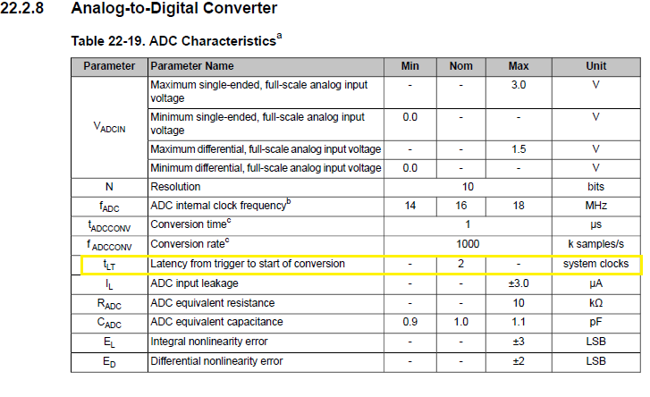
Seems plausible hardware averaging decreases throughput by a factor of the SPS factor would impact the listed conversion time (tADCCONV = 1us).


Example: If 8x over sampling is enabled the conversion time multiplies to 8us or is only the latency from trigger to interrupt (2 SYSCLK's) multiplied by the conversion factor.  

  • Hello BP101

    The hardware averaging does not affect the conversion time, but it affects the latency of the final output from ADC FIFO viz-a-viz the first conversion.

    Regards
    Amit
  • Hi Amit,
    You are saying the FIFO latency from sample trigger to interrupt is a direct multiple of (SYCLKS'S) times the conversion factor but that does not effect the final conversion time?

    Oddly the SW seems to disagree and fails to reload a timer properly if I remove the conversion factor multiplier against total SYSCLKS.
  • Hello BP101,

    I am saying that when hardware averaging is used then the time from trigger to interrupt is ADC Conversion Time for 1 Sample * Hardware Averaging.

    Regards
    Amit
  • Hi Amit

    That seems to elaborate on you first wrote latency was effected. I tried latency only and oddly it works this time, multiplying only the latency (2-SYSCLKS) by the conversion factor (8x). That value dropped from 8160ns to 1160ns multiplying latency alone.

    Your last post seems to agree with my first post example 1us* 8X over sample= 8us total conversion time to interrupt and the latency remains always (2 -SYSCLKS)? One might speculate that latency would also become a multiple of oversamples since the start of conversion is extended out by the total time it takes in the over sample period.

    So you are now saying both latency and conversion time are effected by hardware averaging? Please be specific as the datasheet does not give the method of how the FIFO accomplishes this in any great detail.

  • Hello cb1,

    OK: It is the time from trigger to interrupt that is multiplied 8x times. The conversion is for a sample and that is not affected by Hardware OverSampling.

    Regards
    Amit
  • Hi Amit,
    Ok that works out to some number of (SYSCLK'S). Any easy way to measure time from ADC trigger to actual interrupt or simply multiply (Numb SYSCLK's * 8x= Trig-INT time) . I used GPIO pin to watch time from the interrupt entry up to the point where the values is asserted but want to verify the other time is correct since it gets added for a total sample time.

    The GPIO and scope proved the second time interrupt entry was over timed by more than 100us.
  • Hello BP101

    I think you are on the right track. The easiest on board measurement is to set a GPIO when the timer generates a ADC trigger (enable the timer interrupt as well to set the GPIO high), and then clear the GPIO in the ADC Interrupt Handler.

    Regards
    Amit
  • Hi Amit,

    It is the PWM generator triggering the ADC samples. So how to set a GPIO output level from the ADC or PWM triggers. I know a GPIO can trigger ADC or a timer but don't think it is possible the other way around.
  • Hello BP101,

    Since it is the PWM, you can set the PWM output pin to toggle. Setup a GPIO to toggle 0->1->0 in the ADC Interrupt Handler. By seeing how many PWM pulses you get for 1 ADC Interrupt GPIO pulse, you can get to know the time.

    However do note that if the PWM is running at 1ms interval, then the ADC will take ~8ms (if 8x Over Sampler is used) since the ADC is spending only 1us for conversion and 1ms-1us waiting for the next trigger.

    Regards
    Amit
  • Long ago (on a planet far away) we had similar curiosity.   We devised a (perhaps) tighter method to try and tease out an answer.

    We fed the ADC (single channel) with a linear, monotonic, rising ramp voltage and tuned that ramp frequency to best match our PWM Generator's 20KHz frequency.   Then - in theory - each ADC reading (ranging from 0V to 3V0) will relate the ADC's "conversion time slot" to the PWM trigger. ("PWM_TR_CNT_Load" if not mistaken.)

    The (reasonably) exact "point of measure" proved a curiosity - but not of great (usable) value - as I recall.   (again this was 4+ years past - w/LX4F...)

    [edit] 16:18 CST - thinking a bit more - we subsequently moved from our DAC driven analog ramp to simple, single pulse into the ADC.   Thus "ADC" readings at/about 0 occurred outside of our pulse's (high time) arrival.   By suitably narrowing that pulse width - and then timing the arrival of this pulse (as reported by the ADC's (near) saturation (~4K) reading - a very repeatable (thus (almost) precision) "Where in time" did the ADC's (actual) conversion occur - could be obtained...

    The beauty (if any) of this method was the removal of any latency and/or interrupt delay effects (i.e. it mattered NOT if or when they occurred - what did matter was the capture of a progressively narrowing GPIO pulse - injected into an ADC pin - and then the comparison of the time difference between that "ADC pulse capture" and the entry into the PWM Generator's 20KHz interrupt.)  

    An earlier post suggested the toggle of a GPIO w/in the ADC service routine - which introduces several error sources - each eliminated by our firm's past method...   The (real) proof of the pudding is the ADC's "capture" of a very narrow pulse - and then the relation of that "point in time" against (several) other, known and well time-controlled events...

  • Hi Amit,
    The PWM is three phase 12.5kHz. Yours and CB1 post gives great mind stimulus. My thought is to time GPIO against the falling edge of any pulse following the tallest and two demagnetization pulses. long ago posted photo high lights ADC trigger points in each every other pulse except demagnetization. Those two pules coincide with 1/2 bridge free wheeling diodes and BEMF zero crossing points.
  • Thank you monsieur bp101 for your kind (not self-awarded) Verify.   (cb1 performs a "not quite graceful" jig)

    I'm thicker than a boulder (head-wise, more often now than past) but you may inject that ADC test pulse into (both) an ADC pin AND into a Timer pin - and employ the timer to "time-stamp."    Such provides (another) "relation in time" in the attempt to "tease out" just when - the MCU's ADC "makes its conversion."   It's important that you confirm that your ADC "caught" that narrow, injected pulse - otherwise this is an exercise in futility!   Minus that "proof" I belief all other methods descend to, "witchcraft, wish, hope" - (not that there is (too much) - wrong w/that...)

    Do note - your fetching and subsequent "reading" of that measurement is NOT part of this equation - and to my mind - of less importance.

    By "knowing" - with some exactness - just when the ADC is to make its conversion - you may be able to "quiet" and otherwise exploit measurements occurring in and around that key/critical time slot...

  • Nice thing about storage scope is one can delay the trigger position on either trace and extend the horizontal time base into the region of perceived ADC trigger firings. Triggering scope on the falling edge of delayed PWM pulses and comparing with GPIO rising edge proved most effective. The average sample period at 12.5kHz ended up being at 1660-1680ns. Have to wonder if that sample window changes with PWM frequency changes.

    The thing that surprised me most is the ADC is not triggering with every PWM pulse on Phase 1 test probe. Seeing instead 3 periods of ADC sample interrupts and expecting zero load trigger was occurring with every PWM pulse period. Seems current is not being sampled as often as I had believed it was. That may be due to original code only configured one generator for PWM load count trigger versus having all 3 generators configured to drive an ADC trigger pulse on anyone of them reaching load count zero.

    Any thoughts on why there are only 3 ADC sample period over the entire trapezoidal wave form?
  • Hi Amit,
    >That value dropped from 8160ns to 1160ns multiplying latency alone.
    Odd thing is the scope timings 1660-1680ns ADC trigger to interrupt times appear closer to 1160ns. Perhaps that formula is not very reliable as first believed.
  • Perhaps its me - but I don't believe you're following my (detailed) post's construction and direction!    

    Instead - are you not "wishing/hoping" that your (likely) "ADC interrupt GPIO toggle" has "overlapped" the ADC's actual conversion time-slot?  

    Here's a direct bp quote, "Triggering scope on the falling edge of delayed PWM pulses and comparing with GPIO rising edge proved most effective."   Really - might you explain how, where and why?   What properly defines, "delayed PWM pulses?"   And why is that important?   And your (other measure) "GPIO rising edge" - what is the value/validity of that?   How have you "proven" the value of either?   (I submit you have not!)

    Method I suggested "insures" such "actual moment capture" - method you employed (I suspect) relies upon wish/hope...  (My suggestion - injecting a known, narrow pulse into the ADC - and then noting its proper measure - is the "Gold Standard" - the way you seem to suggest - (minus real detail) provides NO guarantee that you've "caught" the exact moment of conversion!)     Have you "missed" that - or disputed its validity?
     
    Might a 2nd read of my (detailed) post - especially the added/edited portion - aid comprehension?
     
    Again - the method I proposed insures that you're capturing, "that point in time" in which the ADC is actually making its "data capture."   My firm believes (that) time-slot to be of most significance - and not (really) extracted by the (unspecified) method you may be employing...

  • Hello BP101

    I would disagree that the timing window would fall from the ~8us to ~1us. One thing to make sure is that the PWM is not mis-triggering. A good way to ensure the same at every run is to reset the peripherals (ADC and PWM) before enabling the clocks.

    Regards
    Amit
  • Amit Ashara said:
    ...Reset the peripherals (ADC and PWM) before enabling the clocks.

    Right you are (again) Amit - starting (always and only) from "known & proper - initial conditions" is fundamental.

    Our poster continues to kick KISS to the curb - his measurement exercise is likely to be confounded by the variance introduced by the PWM's triggering of the ADC.   My firm (really) searched the "fine manuals" seeking such detail - to no avail.

    KISS would see the early employment of, "ADC_Processor_Trigger" and then an ADC measurement method - as we past detailed.   This eliminates all overhead time-burden (likely) caused by the PWM trigger.

    Our method - injecting a precisely placed, narrow pulse - into the ADC at known & controllable "time-slots" - and then confirming that the ADC "captured" that narrow pulse - is the "most accurate means" my firm found to learn the ADC's "moment of truth!"   (i.e. that point in time when the conversion data was actually acquired)

    Use of the clearer & simpler, "ADC_Processor_Trigger" - along w/the pulse injection method (repeatedly) outlined - complies w/KISS - and the discipline enforced best "sets the stage" for the (far more) complex, "PWM-Triggered" ADC conversion method.   

  • Hi Amit, CB1

    I didn't write this code but am only verifying it is behaving as expected.

     >My firm believes (that) time-slot to be of most significance - and not (really) extracted by the (unspecified) method you (seem) to be employing...

    I wasn't interested in the exact conversion time rather how long it takes from pwm_trg_count_load trigger to actual interrupt and from interrupt to various places in the ADC interrupt handlers SW. Those two BEMF interrupt time factors were according to the programmers notes on the subject, speculate they didn't employ such detailed test methods as CB1 firm did. AKA a bit beyond a quick check and garden variety testes.

    Clarification:  

    One GPIO location uses the combination of both ADC interrupt timings to reprogram the BEMF timer for the (approximated) next zero crossing. How much more KISS does it have to be if we know the PWM generator output causation in the trapezoidal wave form ever pwm_trg_count_load event  The real question, does pwm_trg_count_load occur during the transition of low to high side MOSFET drive (distinct fish hook mid point rising PWM pulse edge) or does the falling edge event seemingly signify pwm_int_cnt_zero. Originally deduced event falling edge was count_load but after some additional thought seems plausible that event occurring at the very end point of fish hook. What say the PWM experts?

    I want to know my PWM DSP signal behavior, sleep with and eat breakfast with it. LOL

    The 3 pulses were due to where the GPIO assert was placed inside the BEMF edge detection SW but later discovered the very same three edges were present in current detection SW period. As a result the ADC SW was only providing export current updates at 3 places in the trapezoidal wave form; beginning middle and end.  That occurs when testing the phase current index (!=) previous phase current index. Setting that index test to (>=) the current sample positions mirroring PWM pulses but the first edges of 12 sample interrupt pulses moves to the center of the trapezoidal wave following it to the end.

    Which is better 3 current export interrupts spaced evenly in the trapezoidal wave form or 12 pulses from center to end?

    Not really sure if the PWM cycle refers to the entire trapezoidal wave form on each phase or the individual PWM pulses in the trapezoidal wave form. Some clarification on terminology would go a long way in understanding ADC phase current samples. Term cycle by cycle current limiting from the BLDC perspective might infer the entire trapezoidal wave. From the MOSFET perspective that might infer gate drive time and DS pulse period avalanche current. The former 3 pulses seem plausible would produce an average BLDC current update where 12 pulse would produce rapid updates center to end of the trapezoidal wave form forcing sudden duty cycle updates in the avalanche current output. Which one is better or safer?

  • Your preference for: deduction ("Originally deduced event falling edge was count_load but after some additional thought...") over a tightly controlled, far more disciplined, experimental procedure - may cause an (on-going) avalanche of misunderstanding.  (i.e. an uncertain foundation is unlikely to yield best results...)

    How do we know exactly when the (mystery laden) "PWM_TR_CNT_LOAD" actually does its job?   (years back - when we searched the fine manuals - neither we nor our talented FAE could make such "deduction" w/certainty - thus our experimental procedure via time-stamped, precisely placed, pulse injection into the ADC arose.)

    Not much more to say/add - I've presented a method - believe it to "rise (far) above deduction" - and readers are free to comment, propose other ways/means - or "deduce" w/out benefit of confirming test/measures...

    As to the gold standard - "Cycle by Cycle current limiting" - that's almost entirely based upon HW (MCU's analog comparator) and monitors each/every PWM driven, current pulse - trapezoidal or other waveform...   Post steers far now from the subject line - Amit (properly) does not like that - I've made my focused contribution and seek to avoid subject's expansion...

  • >Post steers far now from the subject line - Amit (properly) does not like that - I've made my focused contribution and seek to avoid subject's expansion...

    Perhaps not at all since the thread asks how hardware averaging affects conversion time and latency which directly impacts BEMF zero crossings and current limiting. May attempt the timer program to prove PWM edges after understanding what HWA latency is effecting.

    Not sure what you mean by HW analog comparator, the ADC samples shunt voltage on each phase. Have forever expected each pwm_trg_cnt_load coincides with each PWM pulse period but that clearly ain't the case for what ever reason. Plausible HWA seems to delay the total number of pwm_trg_cnt_load events that occur per PWM periods. Otherwise cycle by cycle (PWM period) current limiting isn't actually in play as the MOSFETS are firing many more times than samples being taken. Like I said without ever having a GPIO added in SW the ADC trigger from PWM load would never be exposed for scope inspection.
  • My belief is that you can do (little) to impact the ADC's conversion time. That's (usually) thought of as an MCU ADC's, "aperture" - opening briefly - and digitally capturing the input signal.    Thus - any/all subsequent manipulations (even HW Averaging) cannot influence that. 

    I thought it useful to know just when - in relation to key, other events - that ADC conversion actually occurred.   And time-stamping - by far - trumps "deducing."

    Yours may be a language issue - I doubt "conversion time" extends to include the "post conversion" processing time and averaging - as you attribute.

     You introduced "Cycle by Cycle" - we current limit @ each/every one of those cycles! (such was done long before MCUs moved to this BLDC space - and proved the "gold standard." And to achieve such current monitoring (and limiting - when required) we employ the MCU's Analog Comparator which feeds the PWM Fault Input. (but I've written just that - multiple times past - right here...)

    I stand by the experimental, careful method I described in detail - not so much by (other than factory staff) "deductions."    Without such measurements - and verifications - you build a "House of cards" - do you not?   (I'd avoid the upper floors of any such, "construction.") 

  • >You introduced "Cycle by Cycle" - we current limit @ each/every one of those cycles! (such was done long before MCUs moved to this BLDC space - and proved the "gold standard." By any standard sample latency is more like a soldier MIA..

    Cycle by cycle infers each PWM period is a cycle - you have repeated every cycle is current limited for years. Amit's placement of GPIO checking against PWM strategy proves several things mostly latency in expected samples and SW is current averaging with limiting in the average (qs-bldc) SW/ hardly the gold standard. The gotcha, 3 index pulses all 3 occurring synchronous with the Trapezoidal wave form. However when we configure the current index to track each PWM generators ADC trigger we do get cycle by cycle (12 index pules all center top each PWM pulse ^ cnt_load) but loose sample synchronization with the Trapezoidal all but the center phase. The first phases current samples do start more to the right of the trapezoidal wave form but 12 samples occur nit 3. Not so sure current averaging is bad but perhaps care must be taken in MOSFET selection? I say that because SW as configured can not properly track each PWM period in the MOSFET current avalanche rather only checks the average across the entire trapezoidal wave in 3 repeating and distinct positions (start center end).

    I think the channel reprogram shift between phases has more to do with the current index being changed via GEN 1 interrupt only and a phase delay results for the other two generators. Have tried to configure GEN2&3 for pwm_tr_ cnt_load not seeing any improvement in the phase relationship with 12 pulses.

    Idea comes to mind might can use your timer test. Where each Generator triggers a one shot timer, the interrupt reprograms the ADC sample sequencer current index removing that task from Gen0 interrupt vector. That might keep the index synchronous with the sample latency.
  • BP101 said:
    ...you have repeated every cycle is current limited for years.

    Indeed - and that's because it is absolutely true!   And verifiable - quickly/easily - via peer review.

    This is achieved (as so often noted, here) via (essentially) "pure hardware" means.   No ADC limitation is introduced.   The "Analog Comparator" (either external or w/in the MCU) ALONE monitors each/every PWM impulse - and has the means to, "Cease that PWM Impulse immediately" and of course that occurs each/every PWM cycle!   (thus it qualifies as cycle by cycle)   And - should the PWM frequency alter (either thru intent or hiccup) or the MCU "hang" - the comparator (again either external or w/in MCU) cares not one whit - and continues to (uber effectively) Current-Limit!

    My firm did not invent this method - we did devise a clever & efficient means to exploit the power of the M3 & M4 to simplify, speed, and render this current-limit method more robust.   I've detailed how we've done this - I've no desire to "fit" our success to your "deduced" model.

    If you'd invest (some) time/effort in the experimental method I've detailed I'd bet that you'd observe "variation" in the time delta between PWM Trigger and ADC's (actual) digital conversion.   I've no doubt - the PWM Trigger launches your ADC conversion - with "not so great" precision.   (in fact - iirc - the PWM Trigger is the least precise of all ADC triggers!)

    Note that Amit's initial post - and mine (several back) - have both noted that your "understanding" of ADC's "conversion time" is "non-standard!"   Again any post conversion processing (even your averaging) has zero impact upon the MCU's "ADC Conversion time" (Tc) which is listed as 1uS.   Correct descriptions (usually) yield the best - and fastest results...

    One final point - earlier you noted "2 MCU clocks" as the ADC's "latency."   Yet - a better review of MCU spec reveals that those "2 clocks" are a "typical" value - thus, "Not cast in stone!"   And - the PWM Generator may be placed in, "Edge or Center" mode - which further confounds & complicates (even your) "best deduction" - does it not?

    Perhaps (now) you will accept the need for "hard experimentation & measurement" (in place of (likely) flawed deduction) - to develop (real) understanding...

    Good luck w/your design - there's nothing I can (further) add...

  • >If you'd invest (some) time/effort in the experimental method I've detailed I'd bet that you'd observe "variation" in the time delta between PWM Trigger and ADC's (actual) digital conversion

    Very true since Amit long ago pointed out the ADC is in a different clock domain than PWM generators. Point you seem to argue against is the edge formed during pwm_trg_cnt_load  provides a true scope trigger point and ADC conversion & latency dynamic. Might benefit you to try your storage scopes delay of the trigger point channel B (feature) and you to may discover all is not what has been believed about current limiting. This testing is being derived around the LM3S8971 equipped with 3-INA282 current sensors. The 12 GPIO pulses and ADC samples line up with Hantek current probe and INA282 signals over the entire wave shape but the original SW checks only 3 samples.

    Again the  ADC aperture you speak of was only being tested 3 times during the entire phase wave form generation. Note worthy is the latency calculation time period did not increase with the conversion time factor 2x,4x,8x rather could be greatly reduced. That said, something ain't holding true to deductive reasoning. Most notable as HWA factor value is decreased or set to zero the SW total latency period must be increased or the BEMF timer trigger zero crossings were late and motor would not start.

    The question is why LMI only sampled current 3 times over the entire trapezoidal wave form? The Opamps and INA282 are keeping pace with each PWM pulse but the ADC and SW was not. I think this can be improved greatly to sample each and every PWM pulse as it should be doing with (pwm_trg_cnt_load) yet is not.

    Scope top trace GPIO port - middle INA282 205kHz pulses superimposed over Hantek have same 884us period as GPIO. You can see the first PWM demagnetization pulse in both INA282/Opamps. Otherwise the GPIO would only pulse 3 times with the current index being incremented by only GEN0.


  • BTW: The latency 20us or 2 system clocks in datasheet lines up with pwm_trg_cnt_ld (^ each PWM pulse) is also the time from trigger to sample start based on 0x HWA + 1us conversion time. So the formula is as Amit pointed out and the scope concurs 20us*8x = 160ns+1us=1160us and 1660usns up to the GPIO 1st pulse where SW exports the current calculation.

  • BP101 said:
    the edge formed during pwm_trg_cnt_load  provides a true scope trigger point

    Really - and just how do you (capture) each/every such ADC trigger?   Are you not "guessing/hoping" - exactly when - that ADC trigger occurs?

    Is not that "ADC trigger parameter" set just once - during PWM initialization?   (which precludes your, "toggle of a GPIO" to "mark" that trigger event!)

    I'm betting that you are "hoping/wishing" - that said ADC trigger - occurs in coincidence w/entry into the PWM Interrupt.   And yet there are different modes of PWM output (center, edge - to name just two).   And the latency is not two ADC clocks as you (earlier) wrote - that's just a typical!   So really - other than through our exacting measurement method - how do you "hope" to identify a "true scope trigger point?"   (your words!)

    Thus your "deductions" must include some other means to discern that "exact" trigger time-slot - so that you can (claim) - your "true scope trigger point."

    You may contrast our (past) multiply described tech detail as to how/where we made this attempt against your "true scope trigger point" - yours minus ANY (most necessary) tech detail.   (that key info - left to the reader - really?)

    "Deductions" are unlikely to trump hard measurements - even when deductions are ripe w/hope/wish - even withcraft...

  • BP101 said:
    BTW: The latency 20us or 2 system clocks in datasheet lines up with pwm_trg_cnt_ld

    You continue to, "Play loose w/the facts" do you not?   The ADC runs @ 16MHz (minimum) - not at the System Clock!   And the ADC's latency (listed as Tlc) is clearly described in "ADC Clocks" - NOT system clocks as you promote!

    Worse still - 2, 16MHz ADC Clocks veer far from the bp "claimed" 20µS - do they not?   (62.5nS * 2 - by this reporter's "back of envelope calc.)


    Some attention to detail is required - you're smart enough to know better - might the "house of cards" deserve (some) strengthening/rethink?

  • >Really - and just how do you (capture) each/every such ADC trigger?

    In my opinion you don't need to since each every ADC trigger event occurs center of each (pwm_trg_cnt_ld) bottom trace. By the book ADC trigger is supposed to occur in the center of each PWM pulse exactly 2 system clock cycles later or 40ns @0x HWA, 160ns @8x HWA. The rising edge top trace GPIO moves to changes made in HWA factor values 2x,4x,8x etc.. 

  • Your (post up) appears to have "butchered" your ADC Latency calculation. As you used that to "PROVE" your "deduction of PWM Trigger's actual occurrence/arrival time-slot" - might your "house of cards" require (some) reshuffle?
  • And - let the record note - that you've made NO/ZERO Effort to describe what you believe to be your, "PWM_Trigger!" You are "guessing" what that (may) be - are you not?    And your well justified latency calcs - which "prove your point" seem to (spectacularly) fail when even (briefly) examined...

  • That capture includes the time to GPIO output down in SW from the ADC interrupt entry. The capture shows the GPIO pulse is present at some exact time after that ADC trigger event took place. Given NVIC is play total time from ADC trigger into the ADC interrupt may vary and it does seem to jump ahead jitter exact position seen in the ghost on right.
  • Myself - and staff - cannot parse your writing.

    Which GPIO output?
    What does, "down in SW from ADC interrupt entry mean?"
    How do you "know" when that "ADC trigger event" took place? After all - that's what we're trying to determine - is it not?

    It is becoming too frustrating to continue - you present as "facts" items which (too often) are "hopes/wishes and/or incorrect "deductions.""

    A sound method of experimentation has been (earlier) presented in detail. Rejecting that science - replacing it with "orders of magnitude, erroneous deductions" (i.e. 20µS ADC Latency!) - may not enable your (hoped for) product introduction - anytime soon...
  • I've made the effort to dig up old program notes and can report the following:

    • by monitoring the change in direction bit w/in the appropriate PWM Register we note that most always - while in "Up/Down" count mode - the PWM Trigger does occur (very) near the center of each PWM Interrupt cycle.   (Importantly - and precisely - we mark that time by the repetitive time-stamp entry into the PWM Interrupt - not by that PWM Interrupt's exit time-stamp!)    Thus poster "bp" was mostly correct in noting the "center" - provided that the center is (only) in reference to the occurrence of 2 consecutive, PWM Interrupt entries.  (and not any GPIO toggle - which was positioned at the end of the PWM Interrupt service - which we believe to be the method employed - and which is flat wrong!)   Again - the "center" - as defined here is the, "mid time-point between the ENTRY into 2 successive PWM Interrupts - in no way marked by a GPIO keyed upon PWM Interrupt exit!
    • the determination of the "exact moment" of ADC "digitization" of an impressed voltage appears not so straightforward.   Indeed we can note the entry into the ADC Service - but our measures report that there are time-slot variances here - and the larger the program - the greater the number of higher priority interrupts - the wider these time variances grow. 
    • The post's title is misleading - again the ADC's Conversion Time is noted w/in the ADC specification listing - it is fixed.  (1µS)   Any post ADC processing - to include averaging - in no way impacts the ADC Conversion.   (it could never be specified if such was the case)   A better choice of words may be, "Does xyz impact the time required for the ADC's "processed results" to be ready/available?"  

    We confirmed the above by generating, then placing/applying and time-stamping a narrow pulse - input to several ADC inputs.   Not always was this narrow pulse captured by the ADC (and that pulse was at the exact frequency of the PWM) - which indicates there is indeed variance between PWM Trigger and the actual ADC digitization.   This variation of the exact, ADC digitization time-slot becomes important, as the PWM duty cycle "narrows" - and the time for valid measurement compresses!

    There were variances of the PWM's Interrupt arrival - always delayed - never early.   Multiple other interrupts are active - it's possible that at times - these other interrupts delayed the PWM Interrupt's launch... 

    Our testing was performed upon a 4 year old LX4F MCU board of our firm's design - running @ 50MHz - with a 20KHz PWM frequency.   The variation (delay) in PWM Interrupt arrival was logged and max'ed at 2.4µS (out of a 50µS PWM period - that's 4.8%)  

  • Regarding GPIO repurposed QEI phB for marker. We are told exactly where the ADC trigger event takes place in the text overview. However with dead band enable the B signal is inverted and additional latency is added. Finally have an answer for several of the strange things this review.

    1. If the GPIO output level is inverted in the ADC interrupt handler we get completely different results.

    The PWM generator A pulse is delayed and inverted to make B dead band so the (pwm_trg_cnt_ld) is not on the top or center of each PWM pulse as the text shows in the dang illustration. Can see a GPIO marker pulses current index occurring above each PWM pulse when GPIO is set low on interrupt entry versus high. The exact ADC trigger time measured at the bottom of each PWM pulse @8x HWA is 8.4us. What I needed to know seems to be what I already knew but was told that was not true. The time shows up at the bottom of each PWM pulse. No body said the captures were perfect yet give a foundation to build/learn upon. Discovery is that which needs to be discovered.

    The PWM direction pulse exposed in a register would help greatly anyone at TI care to examine how that might have helped.
  • I screwed up above math 1160ns 16.6us missing a 0 above post should be 11600ns and @8x HWA seemingly measures 16,450ns based on GPIO firing twice at the beginning of ADCIntTrap0.

    The ADC sample time seems to double going from 2x to 8x, HWA makes it appear as if the conversion time changes Ts*8x. Consider the listed 1us conversion time may be wrapped by HW and is listed to correlate with the listed sample time 1000KSPS. Only makes sense that the larger the bit size of the FIFO with higher HWA factors the longer it will take to convert and average the sampled data. After all the samples bits have to go some where in order to average the data in the end. Absent any explanation in text oversampling would seemingly store those data bits in a circular FIFO that's why we decrease in our factor of SPS by the exact amount of the conversion multiplier. Other words how can we have a useful end average if the FIFO dumps the sample data every cycle. Dumping the FIFO wouldn't make any sense so we have to hold all sampled data until the very end to average the total collected. That takes more time

    I no longer believe 1us conversion for every HWA factor than there is a man in the moon, especially when 64x HWA is in play. The HWA exponential sample time can be seen in the PWM load times extending with increases in the HWA factor.

    The stranger thing is the ADC interrupt GPIO markers all line up with every PWM pulse if the entire GPIO toggle is placed at the beginning of the interrupt. That behavior changes when the second GPIO toggle is asserted inside the current index test. We loose cycle by cycle PWM current monitor and move to 3 bit current averaging. The current index is not following every PWM pulse. It seems the C+ language to blame as current Index (>) last index renders 0 GPIO pulses And current index (>=) gives us 12 toggles while current index (!=) gives us only 3 watch points. This may be a job for pure assembler?

  • The problem with the ADC channel selector current index skipping over PWM pulses is exercised after removing the test shown below.

    I suspect the entire (if) clause takes more instruction time than the next current index pulses' arrival time, 79us at 6200 Rpm 12.5kHz PWM. The entry into the ADC interrupt every 79us as the GPIO marker proves the (pwm_trg_cnt_load) is circular after all.

    The good thing is the GPIO marker for ADC current index ends up dead center of each low side MOSFET on time for 7.5- 8us. The current index changes reading the ulPWMEnable register entry to the ADC interrupt. ADC Sample FIFO depth insures the SOA in 1ms duty cycle adjustments performed during the PWM interrupt cycle. Oddly increasing the HWA factor does widens the 3 pulses in the current index yet 3 samples over the entire trapezoidal wave form seems far to sparse to ensure the MOSFET SOA upon sudden duty changes may resort to running on the edge at times.

    // If we have changed phases, calculate the phase current average.
     if(g_ucPhaseCurrentIndex >= g_ucPreviousPhaseCurrentIndex)
    {
    
      Current Calculations 
    }
     g_ucPreviousPhaseCurrentIndex = g_ucPhaseCurrentIndex;


  • BP101 said:
    ADC channel selector current index skipping over PWM pulses is exercised after removing...

    Might you have meant, "excised?"   (i.e. removed)

    What about, "ADC Conversion" - do you continue in the belief that its, "standard definition" must expand to include, "all possible, user selected, post conversion, result processing activity?"   It's been suggested that, "ADC processed Results" better describes what you're after...

  • >Might you have meant, "excised?"   (i.e. removed)

    No - problem is an evil demonic scourge perhaps more traceable to the code shown below. Should one line up real time phase PWM pulses with the GPIO pulse it is not the low side only being compared via the ADC samples, with or without an abated SSI0 reprogram (return). Instead we arrive with a blended cocktail more like an long island ice tea. In those 3 distinct 75us wide sample apertures (ulPWMenable) the GPIO lines up with both rising edge of PWM and falling edge precisely delivering more high side than the projected low side in programmers note.

    No matter if comparing (ulPWMenable) HWREG (MOS &0x01 or &0x04) gives similar results of 3 pulse apertures. The point in all that was to read the current shunt on the low side MOS. The sample index being reprogrammed early in the interrupt assumes the previous sample was previously read. Hence the reasoning behind the perceived need for a (return) at the bottom. The phrase "which came first the chicken or the egg" comes to mind. Higher adjustments of HWA factors calms the fire by pushing the ulPWMenable compare (conversion delay time) over to the right side of (mostly high side MOS time) in the PWM pulse.  

    Will be experimenting to see if placing the reprogram after the post processing gives the expected performance. Perhaps this was serendipity at work.

     static void
    ADC0IntTrap(void)
    {   
    
        GPIOPinWrite(GPIO_PORTC_BASE, GPIO_PIN_7, 0x80);
    
        // Reconfigure the sequence for the next sample period 
        // if a change in PWM output drive state is detected.
         ulPWMEnable = HWREG(PWM0_BASE + PWM_O_ENABLE);
    
        if(ulPWMEnable != ulLastPWMEnable)
        {       
            // If the Low side of Phase A is active, enable 
            // current readings on Phase A analog signal.
            if(ulPWMEnable & 0x2)  //was 0x2-Low or 0x1-High
            {
                ulIPhase = PIN_IPHASEA; // Channel 4
                g_ucPhaseCurrentIndex = 0;
                GPIOPinWrite(GPIO_PORTC_BASE, GPIO_PIN_7, 0x00);
            }
    
            // If the low side of Phase B is active, enable 
            // current readings on Phase B analog signal.
            else if(ulPWMEnable & 0x8)  //was 0x8-Low or 0x4-High
            {
                ulIPhase = PIN_IPHASEB; // Channel 5
                g_ucPhaseCurrentIndex = 1;
                GPIOPinWrite(GPIO_PORTC_BASE, GPIO_PIN_7, 0x00);
            }
           
            // Assume Phase C is active, enable current
            //  readings on Phase C analog signal.
            else
            {
                ulIPhase = PIN_IPHASEC; //Channel 6 0x20
                g_ucPhaseCurrentIndex = 2;
                GPIOPinWrite(GPIO_PORTC_BASE, GPIO_PIN_7, 0x00);
            }
    
    	// Disable the sequence.
    	HWREG(ADC0_BASE + ADC_O_ACTSS) &= ~ADC_ACTSS_ASEN0;
    
            // Reprogram the Phase Current sequence entries.
            ADCSequenceStepConfigure(ADC0_BASE, 0, 1, ulIPhase);
    
            // Save the PWM output state.
            ulLastPWMEnable = ulPWMEnable;
    
            // Enable the sequence and continue processsing ADC 
            // interrupt for the previous sampled phase current.
            // Avoid returning from interrupt after enabling the 
            // sequence stops Watchdog timeouts durring motor start  
            // for any PWM frequecy below 20kHz while in sensorless
            // BEMF commutation mode.
            HWREG(ADC0_BASE + ADC_O_ACTSS) |= ADC_ACTSS_ASEN0;
    }

  • The GPIO marker is not moving the index in the low side MOS samples synchronous with the PWM pulse stream. So the same low side index point in the very same few PWM pulses are always being processed instead of processing a real time current sample in each/every PWM pulse.

    It appears as if the ADC sequencer index is not being reprogrammed synchronous with the PWM generator events. Even though the ADC interrupt GPIO marker is synchronous with each and every MOS low side PWM event.

    IE: We should be seeing a marker pulse inside each/every PWM pulse to indicate the current sample moves in real time.
  • BP101 said:
    We should be seeing a marker pulse inside each/every PWM pulse to indicate the current sample moves in real time.

    Didn't you note this multiple posts back - the ADC only converts upon the "fresh arrival" of a new, motor phase.   Recall the original BLDC SW sought a, "Change in motor phase" to actually "make" the ADC conversion.  When subsequent, PWM generated, ADC triggers arrived - AND - the motor phase was unchanged - the ADC conversion code loop was - by intent - bypassed!  

    Agreed that each PWM cycle (potentially) "triggers" the ADC to convert - but as you've found (and stated here earlier) such ADC conversion only occurs upon a, "Change in motor phase." 

    The BLDC SW you & I reference was written for a (long past) Cortex M3 - perhaps it was not judged (adequate) to manage Ethernet, CAN and "each/every" PWM inspired ADC conversion.

    You may start to see the value (now) of "Independent, Cycle by Cycle" Current Monitoring/Clamping - achieved NOT by MCU SW - but by an Analog Comparator.   (MCU's internal or external)   (has that appeared here, before?)   This provides much needed over-current protection - yet does not "overwhelm" the MCU - with constant, chronic ADC processing.

    As you've migrated to an M4 - you may be able to increase the number of ADC measurements - OR - you can "offload" those ADC measurements to a higher performance (external) ADC - triggered via your GPIO.   (although you still may seriously "load" the MCU)

    An alternative is to program the ADC to "convert" every Nth pulse - w/in the same motor phase - which will lessen the demands upon the MCU - and likely prove adequate to your needs.   You may (even) further experiment by "rejecting" that "first" new phase measure - instead opting for subsequent PWM pulses w/in that same motor phase train...

  • There's a very critical difference with a comparator, it monitors the entire PWM pulse(perhaps minus some blanking) unlike the single point monitored by the a/d. Unlike the a/d it can catch currents that rise quickly within a pulse. Important in the presence of dead shorts.

    Robert
  • Robert Adsett72 said:
    ...comparator monitors the entire PWM pulse (perhaps minus some blanking) unlike the single point monitored by the a/d.  Unlike the a/d it can catch currents that rise quickly within a pulse.

    Very well said Robert.   And we have noted & benefited from the comparator's constant readiness to "current-limit" - which you (interestingly) describe as "monitoring the entire PWM pulse."   (I'd not thought of it that way - but believe we are employing different descriptions of the same (important) functionality.

    Of course the ADC's "measure" is critical too - yet as you & I know/agree - the analog comparator can "fill in the gaps" which the ADC "alone" (used by some here) cannot achieve...   Clearly the proper "blend" of ADC & Analog Comparator - each managing what it does best - provides the best overall motor drive performance.

  • The problem mentioned above post was stemming from reprogramming ADC sequencers inside the interrupt handler. The code was more static and not driven by a real time dynamic moving index in the PMW generators time. The static index 0,1,2 could not sample current across the entire wave form but only in time with the interrupt selected NEXT PWM output. Using all 3 PWM generators to trigger ADC samples in 3 predefined sequencer steps allows the index to be incremented beyond 2. That seemingly allows the exported current calculation to produce more data in the aperture of the 1ms period but on a much wider scale.

    The oddest part was the ulTemp being drained to empty the FIFO at the beginning of the interrupt was being mostly used in the current calculation and the RAW FIFO data to track the maximum in the PWM pulse. Also by creating a dedicated interrupt handler only for phase current measurements the BEMF zero crossings of sensorless commutation was removed from the heap and a single sample for the current. The enhancement now samples all three phases cycle by cycle in real time. Please feel free to make SW enhancements but please do share! 

    Some code changes from above posted current handler.  

    void
    PWMInit(void)
    {
    
       PWMGenIntTrigEnable(PWM0_BASE, PWM_GEN_0, PWM_INT_CNT_ZERO | PWM_TR_CNT_LOAD);
       PWMGenIntTrigEnable(PWM0_BASE, PWM_GEN_1, PWM_TR_CNT_LOAD); 
       PWMGenIntTrigEnable(PWM0_BASE, PWM_GEN_2, PWM_TR_CNT_LOAD);
    }
    
    void
    ADCInit(void)
    {
        /* Configure ADC0 SS1 for PWM module to trigger samples from
         * 3 generator trigger pulses monitoring current on 3 phases.
         * Assign second highest priority to ADC sequencer one. */
        ADCSequenceConfigure(ADC0_BASE, 1, ADC_TRIGGER_PWM0, 2);
        ADCSequenceConfigure(ADC0_BASE, 1, ADC_TRIGGER_PWM1, 2);
        ADCSequenceConfigure(ADC0_BASE, 1, ADC_TRIGGER_PWM2, 2);
    
         /* Configure ADC0 SS1 for PWM module triggered and
          * current monitoring.  */
         ADCSequenceStepConfigure(ADC0_BASE, 1, 0, PIN_IPHASEA);
         ADCSequenceStepConfigure(ADC0_BASE, 1, 1, PIN_IPHASEB);
         ADCSequenceStepConfigure(ADC0_BASE, 1, 2, PIN_IPHASEC);
         ADCSequenceStepConfigure(ADC0_BASE, 1, 3, ADC_CTL_END | ADC_CTL_IE);
    }
    
    void
    ADC0CurrentInt(void)
    {    
    
          /* Check the ADC sequencer for real time phase current
           * if a change in PWM output drive state is detected. */
          ulPWMEnable = HWREG(PWM0_BASE + PWM_O_ENABLE);
    
            if(ulPWMEnable != ulLastPWMEnable)
            {
             /* Disable ADC0 SS1 sequencer and snapshot the captured
        	 * FIFO value in one of the case enabled motor phases. */
            HWREG(ADC0_BASE + ADC_O_ACTSS) &= ~ADC_ACTSS_ASEN1;
    
            // If the Low side of Phase A is active, enable
            // current readings on Phase A analog signal.
            if(ulPWMEnable & 0x02)  //was 0x2-Low or 0x1-High
            {
                // PIN_IPHASEA Channel 4
                /* Increment channel index into the FIFO sampled data */
                g_ucPhaseCurrentIndex ++;
               	// Read the next sample for the current calculation.
                ui16PhaseABC[0] = HWREG(ADC0_BASE + ADC_O_SSFIFO1);
                //GPIOPinWrite(GPIO_PORTC_BASE, GPIO_PIN_7, 0x00);
            }
    
            // If the low side of Phase B is active, enable
            // current readings on Phase B analog signal.
            else if(ulPWMEnable & 0x08)  //was 0x8-Low or 0x4-High
            {
                // PIN_IPHASEB Channel 5
            	   /* Increment channel index into the FIFO sampled data */
                g_ucPhaseCurrentIndex ++;
                // Read the next sample for the current calculation.
                ui16PhaseABC[1] = HWREG(ADC0_BASE + ADC_O_SSFIFO1);
                //GPIOPinWrite(GPIO_PORTC_BASE, GPIO_PIN_7, 0x00);
            }
    
            // Assume Phase C is active, enable current
            //  readings on Phase C analog signal.
            else
            {
                // PIN_IPHASEC Channel 6 = 0x20
            	   /* Increment channel index into the FIFO sampled data */
                g_ucPhaseCurrentIndex ++;
                // Read the next sample step for the current calculation.
                ui16PhaseABC[2] = HWREG(ADC0_BASE + ADC_O_SSFIFO1);
                //GPIOPinWrite(GPIO_PORTC_BASE, GPIO_PIN_7, 0x00);
             }
    
                /* Drain ADC0 Sequencer FIFO of all the captured samples. */
                while((HWREG(ADC0_BASE + ADC_O_SSFSTAT1) & (!ADC_SSFSTAT1_EMPTY)))
                {
                   /* Drain entire SS1 FIFO of all samples
                	* for the current calculation. */
                    ulTemp = HWREG(ADC0_BASE + ADC_O_SSFIFO1);
                }
    		    // Clear any overflow/underflow conditions that might exist.
    		    HWREG(ADC0_BASE + ADC_O_OSTAT) |= ADC_OSTAT_OV1;
    		    HWREG(ADC0_BASE + ADC_O_USTAT) |= ADC_USTAT_UV1;
    
    	            // Save the PWM output state.
    	            ulLastPWMEnable = ulPWMEnable;
    
    	            // Re-enable the sequence and continue processsing ADC
    	            // interrupt for this interrupts sampled phase current.
    	            HWREG(ADC0_BASE + ADC_O_ACTSS) |= ADC_ACTSS_ASEN1;
            }
    
        /* Match the current index to the selected phase current sample for processing */
       ui16PhaseABC[3] = ui16PhaseABC[0] || ui16PhaseABC[1] || ui16PhaseABC[2];
    
    }
    
    // Current calculations:
    
        // Track the (Maximum) phase current reading over the PMW commutation.
        if(usPhaseCurrentMax < ui16PhaseABC[3])
        {
           usPhaseCurrentMax = ui16PhaseABC[3];
        }
           
    
        /* If we have changed phases, calculate the phase current average.
         * Export the current calculation results and update the duty cycle
         * via the PWM zero count interrupt SW generated 1ms periods.  */
        if(g_ucPhaseCurrentIndex != g_ucPreviousPhaseCurrentIndex)  
        {
    
          //  ~~ Current Formulas ~~
          //
            // Calculate the phase current.
            //
            PHASE_CURRENT_CALC(usPhaseCurrentMax, ulTemp, lTemp);
            usPhaseCurrentMax = 0;
    
            /* Track the current index into the sampled data and
             * reset the index when the wave form period expires. */
            if(g_ucPhaseCurrentIndex > 12)
            {
            	g_ucPhaseCurrentIndex = 0;
            }
            g_ucPreviousPhaseCurrentIndex = g_ucPhaseCurrentIndex;
        }


  • >

    IE: We should be seeing a marker pulse inside each/every PWM pulse to indicate the current sample moves in real time.

    The index pulse witness GPIO placement is critical and appears to scan across the entire complex wave from even delaying the B channel trigger in the complex wave form. The GPIO pulse appears to move with the index increment in each sample step so the current 1ms update visual also has varied current peaks (hairs/points) riding the current trace signal. Prior changing the index schema the current trace remained visually flat especially HWA set 2x-8x, all the ADC sample noise disappears.

    Another interesting point is the interrupt marker index no longer captures the 1st demagnetization pulse falling edge. The current shunt amplifier was processing and passing each phases' 1st EMF pulse into the ADC sample data. The very edge of demagnetization tallest 1st pulse was previously being sampled. Now the GPIO marker edge falls just to the right of this rectified phase drive 1st and initial EMF blow back. Being at the beginning of each wave form generation we demagnetize each phase, it seems counter intuitive to sample the 1st pulse at all.

    Setting the index 24 causes instant over current fault. Experiments changes to the index value order to achieve even and distributed PWM current balance may prove beneficial to anyone with a Tektronix current probe. 

     /* Track the current index into the sampled data and
      * reset the index when the wave form period expires. */
     if(g_ucPhaseCurrentIndex > 12)
     {
       g_ucPhaseCurrentIndex = 0;
    
       GPIOPinWrite(GPIO_PORTC_BASE, GPIO_PIN_7, 0x00);
     }
        g_ucPreviousPhaseCurrentIndex = g_ucPhaseCurrentIndex;
    }

  • >Didn't you note this multiple posts back - the ADC only converts upon the "fresh arrival" of a new, motor phase. Recall the original BLDC SW sought a, "Change in motor phase" to actually "make" the ADC conversion. When subsequent, PWM generated, ADC triggers arrived - AND - the motor phase was unchanged - the ADC conversion code loop was - by intent - bypassed!

    Yes it was in my opinion mistakenly bypassing present samples order to reprogram the sequencer. It was not clear to me (ulTemp) was actually the real time sample and not just the FIFO being drained for postmortem reasons. So the current sample data was there but nobody tied it to the current calculation below being the (return) bypassed the real time ADC sample inside the reprogram loop every time so how could it update current using the (ulTemp) drained FIFO. The plausible answer - SW was mostly using the RAW FIFO data most of the time and never had the real time (ulTemp) data to form a min/max current level with every PWM cycle.

    BTW: Usage with incrementing index now moves from 6% idle to roughly 26% at 6300RPM @6 wave form period updates.
  • If you're happy - what's to say/add?

    Two here have described the (unique) ability of an Analog Comparator to monitor (far beyond) the 1µS "aperture" (opening) of the MCU's ADC.   Such Analog Comparator method provides a "protection and control" mechanism which vastly exceeds ADC use - alone... (i.e. w/center-triggered ADC - you are "blind" to some 90%+ of each PWM impulse - are you not?)   And - is it not (likely) that a disturbance often occurs "outside" of your (so very brief) 1µS, conversion aperture?   Can that be good, desirable?

    Might your (recent) move to "hardware averaging" serve to (even further) suppress your ability to capture an over-current impulse?   Some here may note the (apparent) conflict in, "making more measurements" - yet then "averaging away" any critical (deviant) impulses.   Again - your (discounted) Analog Comparator proves absolutely "ideal" for such capture - (as it is not limited to a so brief 1µS aperture {its aperture is unlimited}) and may time-stamp each current "glitch" (and then via an interrupt) log key/critical/associated MCU data - to greatly aid correction.
     
    Increasing the number of such (extremely narrow, point in time) ADC measures may not yield the improved results you seek...   It's unclear "what you sought to improve" - what your (real) measured (improved) results were - and your m.o. for implementing such measures of (that) "hoped for" improvement...

  • One thing about CCP they require something to compare against and are mostly set to detect threshold one level in typical compare situations. Then there is the trigger requirements of the timer etc.. Not sure why you keep insisting 1us when the circular FIFO is set 8x HWA, well explained good reasoning for data sheet listing only 1us. Again the sample time includes the conversion times, the oversample factor plus the latency time yet not fully explained by Amit or datasheet.  Wasn't looking for a new method rather a proper and safer logical method.

    The default SW produced three static apertures (80us wide) index for exported current constrained interrupts, 1ms duty cycle updates of all three PWM generators. We now see over 16.6us each sample plugged into a dynamic 80us scanning index over the entire wave form after the demagnetization pulse. This upgrade provides 36 samples across three wave forms as compared to maybe six samples being captured in the exact same position every time. The static samples were not being trigged but by 1 PWM generator, as a result any current sampled in phase B or C were out of phase with PWM generators 1 and 2. The 1ms  duty updates could at times diverge from the PWM current peaks pushing the FETS into dangerous periods. Possibly not important with a 13Mohm FET the RDK shipped with, far more forgiving than with an 42Mohm FET where those phase shifts from missing triggers generator 1 and 2 where not being captured nor driving interrupts to adjust the duty cycle. Deductively there was a resulting amount of unprotected SOA in the MOSFETS avalanche regions. That's all - need say you can keep doing the same thing in SW expecting different results or try something different with what you already have at hand.

    Better told a movie shows the moving sample index results.

  • BP101 said:
    Not sure why you keep insisting 1us when the circular FIFO is set 8x HWA

    Perhaps because of Amit's initial post - this thread,"The hardware averaging does not affect the conversion time, but it affects the latency of the final output from ADC FIFO viz-a-viz the first conversion."

    And the MCU's data sheet which reveals:

    Again - you cannot alter this "ADC Conversion Time."   We've suggested better name to describe the "post processing" you harness to this spec - but that cannot be called "ADC Conversion Time."

    The use of "personal" definitions most always fails when dealing w/others outside of your immediate group.   (and in your haste you wrote that Tlt was 2 "System Clocks" when the data-sheet lists ADC Clocks.)

    Analog Comparator can be properly set to "Clamp/Limit Phase Current" to user's desired level - we use the MCU's DAC to achieve that (another's M4) and it (alone) provides a robust "full aperture" protection/limiting - unlike your 1µS (so limited, oh so restricted) ADC measure.

    As Robert & I have emphasized - your 1µS aperture into a PWM impulse of perhaps 1mS leaves you essentially, "naked" - does it not?   Attack of those showing interest - but resistant to the bp Kool-Aid (tasty as it is) may not prove best/brightest.   (especially when those helpers/interested are RIGHT!)

  • >and in your haste you wrote that lt was 2 "System Clocks" when the data-sheet lists ADC Clocks.

    See the confusion - LM3s8971 shows same spec as 2 system clocks.

    >As Robert & I have emphasized - your 1µS aperture into a PWM impulse of perhaps 1mS leaves you essentially, "naked" - does it not?   Attack of those showing interest - but resistant to the bp Kool-Aid (tasty as it is) may not prove best/brightest.   (especially when those helpers/interested are RIGHT!)

    Not an attack rather a complete difference of opinion. The (1us) conversion times listed are for sampling at 1Msps without HWA in effect.  The conversion time verified by scope is not 1us @8x HWA rather more a multiple of the rate factor seemingly multiplied by the latency or some other non documented value. The total time it takes in conversion is relative to the size of the FIFO times the number of oversamples. So it seems you are correct to say 1us conversion at 1Msps but it seems the 1us is being multiplied by the factor and who is to say it is not since the entire topic is so poorly documented.

    >Analog Comparator can be properly set to "Clamp/Limit Phase Current" to user's desired level - we use the MCU's DAC to achieve that (another's M4) and it (alone) provides a robust "full aperture" protection/limiting - unlike your 1µS (so limited, oh so restricted) ADC measure

    Perhaps having to add some many extra safe guards are do to improper PWM configuration to the facts I have tried to present here. For example the M3 ADC sample interrupts are occurring at 80us intervals @6300 RPM and the sample aperture widens to nearly 16.6us when HWA is set at 8x proved by posted scope captures. 

    The problem is my scope is only 2 channel so it is difficult to track all 3 PWM generators and the GPIO markers at the same time. Was hoping you might be curious as to how triggering the ADC by 3 PWM generators with dynamic tracking SW triggers might be of benefit, try them out and post some captures. My opinion is the MOS should mostly be protected by adjustments in the duty cycle, that is what MOS-SOA is all about. BTW the entire wave time at 6300 RPM is only 1.5ms and the new SW checks (each) phase at 4 positions without the original added phase shifts in the mix.  Seemingly there is no SW reason the PWM generator can not quickly adjust the duty cycle fast enough in next 1ms tick to protect the MOS. Doesn't the clearing of the ADC interrupt then allow the Cortex to move ahead read buffering the current measurement in each 80us pulse, adjust said current in the very next 1ms period. I think it is safe to interrupt by each generator count zero count and improve the attack of PWM duty cycle updates. Seems the original intent of RDK/SW was purely for demonstration.

    Do agree 100% with CB1/Robert a comparator is a must for PWM generator faults that might occur yet that is not the reason for this SW modification. The goal is to adjust PWM duty cycle to keep the MOS in the SOA specification. Again that aspect in SW was easily over looked being the RDK was using 13Mohm MOS. Great for demonstration purposes not so great for other.

  • BP101 said:
    it seems you are correct to say 1us conversion at 1Msps but it seems the 1us is being multiplied by the factor and who is to say it is not

    No cannot agree - again as Amit & the MCU's spec plainly state - the ADC Conversion Time "IS - and Shall REMAIN" at 1uS!   You cannot alter that.   Your subsequent "read" of ADC data will extend the time from "Conversion ordered" - but that (extra, post-conversion, MCU processing is not defined as ADC Conversion!)   Note that Amit works (presently) in the industry - and I (past) worked similarly - yet you "hold" to your "re-write" of "ADC Conversion."  

    I made the time/effort - earlier here - to greatly detail our (past) vendor FAE sanctioned experiment - in which we injected unique analog levels into the ADC - for precisely timed periods - and this effort (not deduction) confimed the 1µS which you so struggle to resist.   (and/or rename - to your purposes...)

    Pardon but you are incorrect.   Experimentation as we detailed will assure you - deduction - not so much...

    BP101 said:
    the sample aperture widens to nearly 16.6us when HWA is set at 8x 

    Again No!   The ADC Conversion aperture remains at 1µS.   The time to add post conversion processing adds to this - yet does not fall under the, "ADC Conversion" umbrella!   (how could it - no number could then be provided as any/every post-process would have to be listed!)  Again - you are using tech terms incorrectly.   (and quite persistently!)

    BP101 said:
    how triggering the ADC by 3 PWM generators with dynamic tracking SW triggers might be of benefit, try them out

    Why do you believe this bp101 idea has merit?   Using just (plain Vanilla) "PWM0 Gen" causes all Six Power FETs to properly sequence - does it not?   (i.e. has for our tech firm - rather well - for past 6 years!)  As PWM Gen_0 is responsible for just TWO FETs - it must be that the two other PWM Gens are performing - as the FOUR other FETs perform nicely.   (Might you have missed this?)  

    And our (independent) Allegro hall-effect current sensors (running essentially vanilla LMI SW) report a fine balance from FET to FET - and from motor Phase to motor Phase - and have never "switched" beyond PWM Gen_0.  Might you have "forgotten" that the 3 PWM Generators are "SYNC'ED" - and thus this bp101 "invention" is w/out (much) benefit?   If you disagree - what then is the merit of such PWM "syncing" - do not all vendors provide for such.   (and few (none) employ the technique one here describes...)