This thread has been locked.

If you have a related question, please click the "Ask a related question" button in the top right corner. The newly created question will be automatically linked to this question.

TM4C123GH6PM- 24Bit external ADC SPI Communication (Missing data or Getting wrong data)

Hello Everyone

I designed a board that gets 24 Bit ADC data from external ADC using SPI communication. SSIClk runs on 8MHz and my MCU sends 4 MHz clock from PWM pin to ADC clock pin input and output data of external ADC is 3.4 kbps. I use Freescale SPI Mod(1,1) four wire communication. 

I sample 50Hz pure sin wave. After proper communication, I can get 24-bit ADC data. MSB bit is signed bit in 24-bit frame. But sometimes I get wrong data or I missing data. I keep ADC data in one test buffer to observe my sine wave. As you can see in below picture, ADC data suddenly drops to minus value and continue with it.

Y-axis is RMS value of 50 Hz pure sine wave. It is only per some scale of raw 24 bit ADC data.

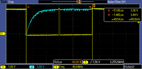
I checked my Chip Select signal which initiates and teminates communication between ADC on oscilloscope. It is as expected. 

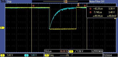
I get ADC data with interrupt. I also checked it. It is as expected too. I dont know where I'm going wrong. 

Any help will great for me.

Thanks in advance

  • How are you setting the time between samples? Did you record a time stamp with each data point? If not, that is the the first or second step I would take.

    The first, if I could, would be to place a logic analyzer or 'scope on the chip select and set the trigger for missing pulses.

    Robert

  • Hello Robert

    I read ADC data and observe these data like below. Chip select signal is directly related with Data Ready Interrupt comes from ADC. I make CS high when I get falling edge from Data Ready pin and after reading I make CS low.

    void GPIOPortE_Handler(void)
    {

    if(GPIO_PORTE_RIS_R&0x10) // ADC Data Ready Interrupt
    {

    GPIO_PORTE_ICR_R = 0x10;
    GPIO_PORTE_IM_R &= ~0x30;

    for(counter=0;counter<3;counter++)
    {
    ADC1Data[counter] = Read_ADC1(counter);
    ADC1Data_24bit[counter] = ADC1Data[counter]<<8;
    }

    ObserveDataADC1_CH1[FallingEdges] = (ADC1Data_24bit[0] / 256) * fixed;
    ObserveDataADC1_CH2[FallingEdges] = (ADC1Data_24bit[1] / 256) * fixed;
    ObserveDataADC1_CH3[FallingEdges] = (ADC1Data_24bit[2] / 256) * fixed;

    FallingEdges++;
    if(FallingEdges == 300)
    {
    FallingEdges = 0;
    }

    GPIO_PORTE_IM_R |= 0x30;

    }
    }
  • Hello Serkan,

    Can you please share the configuration of SSI and the Read_ADC1 API that is being called in your interrupt handler?

    Regards
    Amit
  • how are you controlling the timing? Are you running continuous conversion?

    You absolutely need to get some time information in your data. A time stamp with your data points would be a good start.

    The first thing you need to determine is the characteristics of your sampling. You probably also need measurements of your interrupt trigger and your chip select. Particularly if you are doing continuous conversion the timing relationships are going to be critical.

    Robert
  • Hello Serken,

    In the CCS plotter what are the parameters that have been given before the plotting tool is invoked

    Regards
    Amit
  • Hello Amit and Robert

    My SSI config and ReadADC function code are in below. I checked Data Ready pulse on scope and its period is as expected. It is same with output data rate of ADC frequency. 

    In fact, I am not reading ADC data continously. For getting  one 24 bit data, I make CS high to low. I am repeating same process for every data reading. 

    I tried now in continous mode,I send only one CS signal to read 3X24 bit. Problem remains same.

    void SPIInit(void)
    {
    SYSCTL_RCGCSSI_R |= 0x01; // Activate SSI0
    SYSCTL_RCGCGPIO_R |= 0x01; // Activate PortA
    while((SYSCTL_PRGPIO_R&0x01) == 0){}; // Ready?
    GPIO_PORTA_AFSEL_R |= 0x3C; // Enable Alt Function on PA2,3,4,5
    GPIO_PORTA_DEN_R |= 0x3C; // Configure PA2,3,4,5 as SSI
    GPIO_PORTA_AMSEL_R = 0; // Disable Analog Functionality on PA
    SSI0_CR1_R = 0x00000000; // Disable SSI, Master Mode
    SSI0_CPSR_R = 0x02; // 18 MHz SSIClk, SSIClk(8MHz) = SysClk(80MHz) / CPSDVSR * (1 + SCR)
    SSI0_CR0_R &= ~(0x0000FFFF); // Clear Related Bits
    SSI0_CR0_R |= 0x000004C7; // SCR = 0x04 , SPH = 1, SPO = 1 Freescale Mode, DSS = 8-Bit Data
    SSI0_CR1_R |= 0x00000002; // Enable SSI
    }

    unsigned long Read_ADC1(char adress)
    {

    a = 0x0000;
    ADCdata = 0x00;

    clrbit(ADC_CS1,0); //ADC Chip Select
    a = SSI0_DR_R; // Dummy Read
    read_adress = (adress<<1);
    read_adress |= 0x41;
    SSI0_DR_R = read_adress ;

    a = SSI0_DR_R ; // Dummy Read

    if(adress<3)
    {
    SSI0_DR_R = 0; // Write SPIBufffer. Sets TX Flag, if not done read will not clock.
    while((SSI0_SR_R&SSI_SR_RNE)==0){}; // Receive FIFO Not Empty
    ADCdata += SSI0_DR_R;
    ADCdata = (ADCdata<<8);
    SSI0_DR_R = 0;
    while((SSI0_SR_R&SSI_SR_RNE)==0){}; // Receive FIFO Not Empty
    ADCdata += SSI0_DR_R;
    ADCdata = (ADCdata<<8);
    SSI0_DR_R = 0;
    while((SSI0_SR_R&SSI_SR_RNE)==0){}; // Receive FIFO Not Empty
    ADCdata += SSI0_DR_R;
    }
    setbit(ADC_CS1,0);
    return(ADCdata);
    }

  • Hello

    I realized on scope that sometimes CS signal goes wrongly low to high and after it goes high-to-low as you can see in below scope screen. This happens in continous read mode. Normally one CS signal should be in line when DR falling signal is sensed.

    Normally It looks like below 

  • Serkan,

    That's not the question I asked. Let me try a third phrasing.

    How are you triggering the a/d to start a conversion?

    Robert

  • 1 time stamp your data and plot using time as the x axis. This plotting versus number of conversions is a dangerous shortcut right now
    2 what is the blue trace?

    Robert
  • Hello Robert

    Firstly Blue trace is data ready signal of ADC. Yellow one is Chip Select signal.

    Secondly ADC triggering starts with the interrupt. This interrupt is the falling edge of Data Ready pulse of ADC. When I get falling edge from Data ready pulse, I make chip select of ADC low and thus I trigger the ADC conversion. After I get 3X24 Bit ADC value from ADC, I make Chip select signal high.

    As you can see in graph, sample data between two sin wawe top is 65 sample. I get theoretically 3255kbps. It means frequency of my sin wave = 3255 / 65 = 50.07 Hz.

    Serkan
  • Hello Serkan

    Looking at the snapshot it seems that a stray interrupt is being sensed on the RDY. Can you try increasing the Pull Up Strength so that RDY line rises sharply, or clear the interrupt of the GPIO after the SSI Data has been processed in the interrupt handler

    Regards
    Amit
  • Hello Amit

    I moved GPIO_PORTE_ICR_R = 0x10; line after SSI data has been processed but problem is not solved.

    I dont know how I can increase pull-up strength of data ready pin. 100K pull up resistor tied to VCC in data ready pin. 100K value is suggested in datasheet of ADC. Do you think missed data or problem that occurs in plot ADC data graph is related with this wrong chip select problem ?

    Serkan
  • Hello Serkan

    As we could see in the scope snapshot, that there were 2 data reads from the TM4C12x device when the RDY pin toggled only once, unlike the customary one SSI Read per RDY pin toggle, my suspicion was on the fact that the interrupt handler was being invoked twice for one RDY pin toggle which would also be indicative that there is some rise glitch causing the interrupt handler to be invoked.

    As Robert suggested, it would be good to time stamp the data captures and see if the time stamp show that the samples which are being corrupted are due to twice back-2-back sampling. Then we would need to check what happens from the ADC when a CPU reads data without a RDY pin toggle.

    Regards
    Amit
  • 1: Blue trace. I was afraid of that. That is a problem, that rising edge is way too slow. You either need a Schmitt trigger buffer or a stronger pullup if is open collector or both.

    2: When the data ready fires the conversion is already complete. Then you read it. You need to describe how you tell the a/d to start the conversion.

    3: Use a timestamp. You MUST, absolutely MUST, prove your sampling rate. Do NOT assume it like this. Timestamp and calculate not only average but min and max. Ultimately you should do this for an extended period of time, say 24 hours for convenience. Best to get a histogram so you may need two measurements, one to get the range and the other to fill histogram bins. I say this since so far I see no reason to think there is a uniform sampling frequency.

    Robert
  • Serkan, are you sure about the 100k? That seems very weak.

    Robert
  • Serkan said:
    100K pull up resistor tied to VCC in data ready pin. 100K value is suggested in datasheet of ADC

    Can you give the part number of the ADC and/or a link to it's datasheet?

    [Reading the thread I have been unable to find a mention of which external ADC is being used]

  • Hello

    I am sure about 100K. It seemed also so weak to me. I changed now to 4K7 and data ready signal is sharper now as you can see in below pic

    ADC is MCP3919 3 channel 24 Bit ADC. Data ready sharpness problem solved but  reading problem still continues. 

  • Better but still too slow, I think. I think you need a Schmitt trigger buffer, and the other questions are still outstanding.

    Robert
  • Hello Robert

    Sorry I misunderstood you. I said before how I start reading of ready ADC data. Actually I dont start ADC convertion. If I send MCLK of ADC from my MCU PWM, it continously samples data in certain sample rate and in every DR pulse, I only read it.
  • Okay, so conversion is continuous and you are trying to keep pace with your reading. That does change the possible errors.

    You need that timestamped data and I suspect you need to clean up that data ready signal

    Robert
  • Hello Robert

    What do you mean in "timestapped data".Do you think my reading technique is wrong ?
  • In addition to the good advice provided by Robert & Amit - and in light of the (just arrived) revelation that you are continuous clocking the ADC via the MCU's PWM signal - can that PWM signal be (fully/properly) released from your, "suspect list?"   (your scope's 3rd channel should monitor the PWM output - which clocks your ADC - to establish it's "alibi.")

    Another point - we see 2 full sine wave periods prior to your signal's, "steep dive."   Would it not prove useful to extend your trace time-span - and determine if that "steep dive" occurs consistently - and (possibly) at a regular rate?   (such may indicate an overflow or some form of "disorder" in your ADC clocking.)

    I noted from square one - yours is a 24 bit ADC - and those require very, very special pcb layout, signal routings, and most proper decoupling and powering.   Is your's a "Pro" (factory) board?   If homemade - please tell us it's not on a breadboard - or worse.

    The fact that your graph reveals (at least to me) two apparently good measurement cycles - and then goes "haywire" - leads me to doubt your clocking or perhaps even your MCU's ADC buffer strategy and/or implementation.   My quick read could not find that detail - may prove useful...

    As always - your "need" for 24 bit conversion would be of interest...

  • Serkan, I mean that every time you record data you also record the data, you also record the time you read it from the a/d. You can use a free running timer and get good resolution. You need to do this and do it over as extended period of time as you can.

    Currently you do not know if you are sampling regularly or not. I suspect not.

    You have to determine what is happening with your sampling. You may need to check your plotting as well. Best is to fill a buffer and then dump the data to your local PC to analyze.

    I suspect your sampling is less regular than you think it is.

    Robert
  • Concentrate not on solving the problem but rather determine what the problem actually is

    Robert
  • Indeed, it's rare for a signal to merit even 10 bits. Although usually 24 bits is about dynamic range rather than accuracy. I've often seen them used in designs in liu of an amplifier.

    Robert
  • Dynamic Range! Again Sir - you prove the master. (although finding something "dynamic" w/in 50Hz seems huge stretch...)

    I remain (hopeful) that my observation of TWO Good cyclic measures prior to "Monsieur Le Disaster" will prove fruitful. (cb1 gotta get (something) right!)
  • Serkan said:
    I am sure about 100K. It seemed also so weak to me. I changed now to 4K7 and data ready signal is sharper now as you can see in below pic

    On reading the MSP3919 datasheet, the Data Ready pin is described as:

    The data ready pin indicates if a new conversion result is ready to be read. The default state of this pin is logic high when DR_HIZ = 1 and is high-impedance when DR_HIZ = 0 (default). After each conversion is finished, a logic low pulse will take place on the data ready pin to indicate the conversion result is ready as an interrupt. This pulse is synchronous with the master clock and has a defined and constant width.

    The default state of the DR_HIZ bit bit in the Status and Communication Register is zero. If the DR_HIZ bit is written as a one by the TM4C software, then the Data Ready output will be driven high by the ADC which should give a sharper edge without having to adjust the pull-up resistor.

  • Serkan said:

    unsigned long Read_ADC1(char adress)
    {

    a = 0x0000;
    ADCdata = 0x00;

    clrbit(ADC_CS1,0); //ADC Chip Select
    a = SSI0_DR_R; // Dummy Read
    read_adress = (adress<<1);
    read_adress |= 0x41;
    SSI0_DR_R = read_adress ;

    a = SSI0_DR_R ; // Dummy Read

    if(adress<3)
    {
    SSI0_DR_R = 0; // Write SPIBufffer. Sets TX Flag, if not done read will not clock.
    while((SSI0_SR_R&SSI_SR_RNE)==0){}; // Receive FIFO Not Empty
    ADCdata += SSI0_DR_R;
    ADCdata = (ADCdata<<8);
    SSI0_DR_R = 0;
    while((SSI0_SR_R&SSI_SR_RNE)==0){}; // Receive FIFO Not Empty
    ADCdata += SSI0_DR_R;
    ADCdata = (ADCdata<<8);
    SSI0_DR_R = 0;
    while((SSI0_SR_R&SSI_SR_RNE)==0){}; // Receive FIFO Not Empty
    ADCdata += SSI0_DR_R;
    }
    setbit(ADC_CS1,0);
    return(ADCdata);
    }

    In the Read_ADC1 function, the dummy read from SSI0_DR_R after writing the ADC Control Byte doesn't wait for the receive FIFO to be non-empty before attempting to read the dummy byte.

    There may be a race-condition where the Read_ADC1 function gets the reads from the ADC out of sync.

    Suggest changing the Read_ADC1 function to add a check for the receive FIFO being non-empty before the dummy reads:

    unsigned long Read_ADC1(char adress)
    {
    
        a = 0x0000;
        ADCdata = 0x00;
    
        // Flush SSI FIFO of any stale receive data
        while((SSI0_SR_R&SSI_SR_RNE)!=0)
        {
            a = SSI0_DR_R ;
        }
    
        clrbit(ADC_CS1,0); //ADC Chip Select
        read_adress = (adress<<1);
        read_adress |= 0x41;
        SSI0_DR_R = read_adress ;
    
        while((SSI0_SR_R&SSI_SR_RNE)==0){}; // Receive FIFO Not Empty
        a = SSI0_DR_R ; // Dummy Read to clear undefined receive data during transmission of Control Byte to ADC
    
        if(adress<3)
        {
            SSI0_DR_R = 0; // Write SPIBufffer. Sets TX Flag, if not done read will not clock.
            while((SSI0_SR_R&SSI_SR_RNE)==0){}; // Receive FIFO Not Empty
            ADCdata += SSI0_DR_R;
            ADCdata = (ADCdata<<8);
            SSI0_DR_R = 0;
            while((SSI0_SR_R&SSI_SR_RNE)==0){}; // Receive FIFO Not Empty
            ADCdata += SSI0_DR_R;
            ADCdata = (ADCdata<<8);
            SSI0_DR_R = 0;
            while((SSI0_SR_R&SSI_SR_RNE)==0){}; // Receive FIFO Not Empty
            ADCdata += SSI0_DR_R;
        }
        setbit(ADC_CS1,0);
        return(ADCdata);
    }
    

  • Hello Friends

    Firstly thanks for suggestion on code Chester. I added your code line suggestions to my project.

    I observed my PWM signal that goes to ADC clock input. It seems OK. But this PWM signal is suspicious for me. Because I have a jumper on PWM line. When I remove jumper my ADC data buffer remains with last data sampling and remains with this last data. When I plug jumper again, It takes new measurements into buffer and refresh yourself. 

    My PCB is factory made by the way corresponding to CB1's question.

    It looks like my graph. Because in my graph sin wave firstly seems normal  then there are missed data and after it continous with new data suddenly. Maybe there can be a problem with PWM signal that I can not see.

    I will record a  time stamp with each data point. I will do Robert's suggestion.

    Serkan

  • You've not (really) followed my suggestion to extend your number of data captures - so that any, "regularity and/or repetition" of those "bad data reads" - is revealed!

    Your writing suggests that your pwm signal path (interconnection) - between MCU and external ADC - may not be "short/sweet" - which is ALWAYS the requirement of any high resolution ADC.   Also - your report, "PWM signal that goes to ADC "seems OK"" is not especially convincing.   As past suggested - channel 3 of your scope should monitor your (critical) ADC clock (aka your MCU's PWM signal) - should it not?   Usually - but not always - that clock duty cycle should be close to 50% - and should "rise & fall" to specification and that signal line should be "free" from any other devices, routings or interconnects.   (other than the one between MCU & ADC) 

    The powering of your "factory made" ADC board must be proper (sufficient & fully bypassed) and w/in ADC board's spec.  

    Should your PWM signal deviate from the ADC's spec the issue you report is far more understandable. (and correctable.)

  • That certainly explains the 100k Chester.

    Robert
  • As cb1 suggests, verify that the pwm you produce is within the a/d's clock spec.

    Time stamping will, I think, help. If nothing else it will confirm the presence of a sampling problem, or refute the likelihood.

    Keep in mind that with the removal of the jumper you have reproduced the symptoms but it may be that the symptoms occur due to an unrelated cause.

    Robert
  • Hello

    I am sure about PWM clock is with in ADC spec. I produce 3.3MHZ master clock and 0.8MHz sampling frequency in it. It ADC supports 4 MHz max sampling frequency and16MHz max. master clock
  • Serkan said:
    I am sure about PWM clock is with in ADC spec.

    That is likely true (sometimes)!   But what happens at the point when your conversion accuracy is lost?   If you've "measured" the PWM clock when, "All is well" that may not be sufficient - is that not so?

    Again - your measure of the PWM clock - THROUGH the moment of data error - seems easiest & fastest.   And - this (indirectly) may accommodate poster Robert's good suggestion to "time-stamp."    (i.e. should the PWM clock vary or otherwise deviate - your time-stamps will be directly impacted.)

    Now the greater complexity appears w/in the MCU & your management of the SPI - but w/"uncertain ADC clock rate" - your time-stamps are doomed.   (and they may also be impacted by MCU mishandling - yet monitoring of the PWM clock proves far faster/easier - and should warrant a first order (immediate) inspection.)  

    May I ask poster Robert to comment upon (another's) suggestion of, "race?"   To my mind - the fact that 2.5 full ADC cycles evidence "No race" reduces "race" as a primary cause.   (unless the race slowly/gradually "builds" - and only then - wreaks its havoc.)

  • While I don't think that the noted race would show up as noted (I think you'd see something stranger) it does need to be fixed. And I could well be wrong, I've spent no time determining what you should actually see in that event.

    Proceeding with a blind read is hard to justify though w/o careful study of the timing and with the sure knowledge that the overhead of checking is an issue.

    Robert
  • Hello Friends

    After 2 day hard working on this issue, after changing only test buffer size to certain scale of 50 Hz sampling size, problem solved. All problem was related with my plot settings. 

  • There's a lesson here - "Dummy Data - of known & easily recognizable values" - should be employed prior to feeding (real) data into the plot.

    Unresolved is the initial, unwanted, "device self-read" which remains outside your "command/control."
  • Don't be too quick to declare 'problem solved' Serkan. Your tests showed you have an issue with double reading and you need to verify that is not still an issue and that you do not get any skipped or delayed readings. You need time stamps (or some equivalent) and over an extended period of time to show that. You may need to do some preprocessing of time stamps in order to deal with this w/o large buffers.

    Robert
  • Robert Adsett said:
    Don't be too quick to declare 'problem solved'

    Indeed - as listed - other items (surely) lurk.   Plot failure id is one symptom - not a likely cure.

    Famed, unearned, "Self-Awarded Verify" has yet to appear - good that...

  • Hello Friends

    I have another question to you. My code does not enter to while(1) loop after a short time in the starting. I do not use Watchdog timer. My ADC reading time is shorter than data ready interrupt pulse. I dont why my code does not enter to While(1) loop.

    Serkan
  • Serkan said:
    My code does not enter to while(1) loop after a short time in the starting.

    Your code reveals three "while" loops - does it not?   Your identification of the specific "while loop" which remains un-entered proves helpful.

    As your code fails to reach that point - what has your debugging revealed as to "hang point?"

    Have you made code changes or HW changes (beyond the pull-up value) which may have launched this (new?) issue?