Other Parts Discussed in Thread: TM4C1294NCPDT, EK-TM4C1294XL
Hello everyone, I am back with a question regarding SSI3/SPI functionality on TM4C1294NCPDT; I am working on the EK-TM4C1294XL evaluation board.
I have built an add-on card that sits on connectors X6 and X7 of the EK-TM4C1294XL board. On this card, I have attached a connector where I attach an SPI slave device. (The devices I use are proprietary and I cannot give any information about them, except for an important detail that I will discuss below.)
In my firmware, I have inserted several switch()-case()... decision trees to make it work with all kinds of SPI devices that I want to test. What I am presenting below is the function that initializes SSI3 as SPI / Mode 0 (using Port Q and having ~CS on a GPIO line, PQ1):
// InitSPI(uint32_t SCLK)
//
// Configures SSI3 in master Freescale (SPI) mode using polling method.
// Uses PQ1 to drive the ~CS line.
void InitSPI(uint32_t SCLK)
{
    uint8_t pui8DataRx[10]; // local variable for flushing the SSI/SPI RX buffer

    // The SSI3 peripheral must be enabled for use.
    //ROM_SysCtlPeripheralEnable(SYSCTL_PERIPH_SSI3);

    // For this example SSI3 is used with PortQ[0:3].
    // GPIO port Q needs to be enabled so these pins can be used.
    ROM_SysCtlPeripheralEnable(SYSCTL_PERIPH_GPIOQ);
    ROM_GPIOPinTypeGPIOInput(GPIO_PORTQ_BASE, GPIO_PIN_3);	// MISO - configure it as GPIO input
    ROM_GPIOPinTypeGPIOOutput(GPIO_PORTQ_BASE, GPIO_PIN_2);	// MOSI - configure it as GPIO output
    ROM_GPIOPinTypeGPIOOutput(GPIO_PORTQ_BASE, GPIO_PIN_0);	// SCLK - configure it as GPIO output
    ROM_GPIOPinTypeGPIOOutput(GPIO_PORTQ_BASE, GPIO_PIN_1);	// ~CS - configure it as GPIO output
    CS_High();	// ~CS - set it to logic HIGH

    pinType = GPIODirModeGet(GPIO_PORTQ_BASE, GPIO_PIN_1);	// ~CS
    pinType = GPIODirModeGet(GPIO_PORTQ_BASE, GPIO_PIN_0);	// SCLK
    pinType = GPIODirModeGet(GPIO_PORTQ_BASE, GPIO_PIN_2);	// MOSI
    pinType = GPIODirModeGet(GPIO_PORTQ_BASE, GPIO_PIN_3);	// MISO

    // The SSI3 peripheral must be enabled for use.
    ROM_SysCtlPeripheralEnable(SYSCTL_PERIPH_SSI3);

    // Configure the pin muxing for SSI3 functions on port Q0, Q2 and Q3.
    // This step is not necessary if your part does not support pin muxing.
    GPIOPinConfigure(GPIO_PQ0_SSI3CLK);	// SCLK
    GPIOPinConfigure(GPIO_PQ2_SSI3XDAT0);	// MOSI
    GPIOPinConfigure(GPIO_PQ3_SSI3XDAT1);	// MISO

    // Configure the GPIO settings for the SSI pins.  This function also gives
    // control of these pins to the SSI hardware.  Consult the data sheet to
    // see which functions are allocated per pin.
    // The pins are assigned as follows:
    //      PQ3 - SSI0Rx
    //      PQ2 - SSI0Tx
    //      PQ1 - SSI0Fss
    //      PQ0 - SSI0CLK
    ROM_GPIOPinTypeSSI(GPIO_PORTQ_BASE, GPIO_PIN_3 | GPIO_PIN_2 | GPIO_PIN_0);

    // Configure and enable the SSI port for SPI master mode.  Use SSI3,
    // system clock supply, idle clock level low and active low clock in
    // Freescale SPI mode, master mode, and 8-bit data.
    // For SPI mode, you can set the polarity of the SSI clock when the SSI
    // unit is idle.  You can also configure what clock edge you want to
    // capture data on.  Please reference the datasheet for more information on
    // the different SPI modes.
    ROM_SSIDisable(SSI3_BASE);	// Disable the SSI3 module to configure it
    ROM_SSIConfigSetExpClk(SSI3_BASE,
    			g_ui32SysClock, // this is a global variable to set system clock frequency
    			SSI_FRF_MOTO_MODE_0,
			SSI_MODE_MASTER,
			SCLK,
			8);

    ROM_SSIEnable(SSI3_BASE);	// Enable the SSI3 module.

    // Read any residual data from the SSI port.  This makes sure the receive
    // FIFOs are empty, so we don't read any unwanted junk.  This is done here
    // because the SPI SSI mode is full-duplex, which allows you to send and
    // receive at the same time.  The SSIDataGetNonBlocking function returns
    // "true" when data was returned, and "false" when no data was returned.
    // The "non-blocking" function checks if there is any data in the receive
    // FIFO and does not "hang" if there isn't.
    while(ROM_SSIDataGetNonBlocking(SSI3_BASE, (uint32_t*)&pui8DataRx[0]))
    {
    }

    // Last, initialize number of SPI transfers to zero
    ui32SPITransfers = 0;
}
Below are some information that I can share about the SPI devices that I am trying to test. Both devices have been tested and found to be functional using another, third-party measurement system.
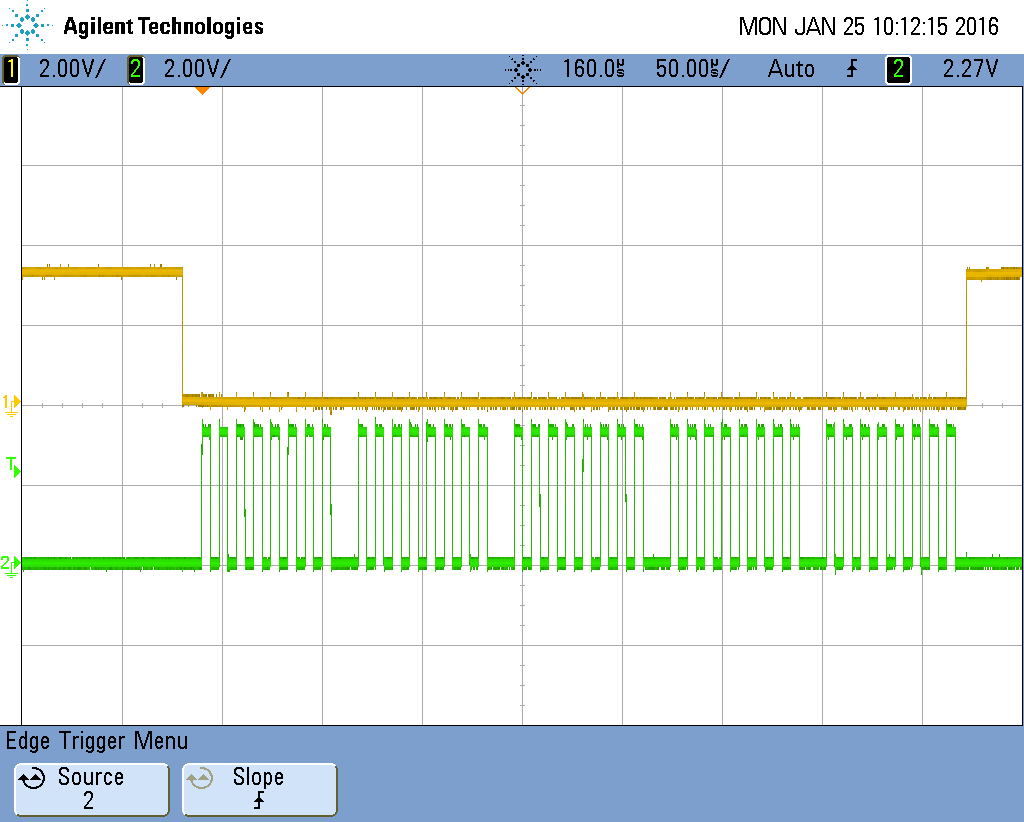
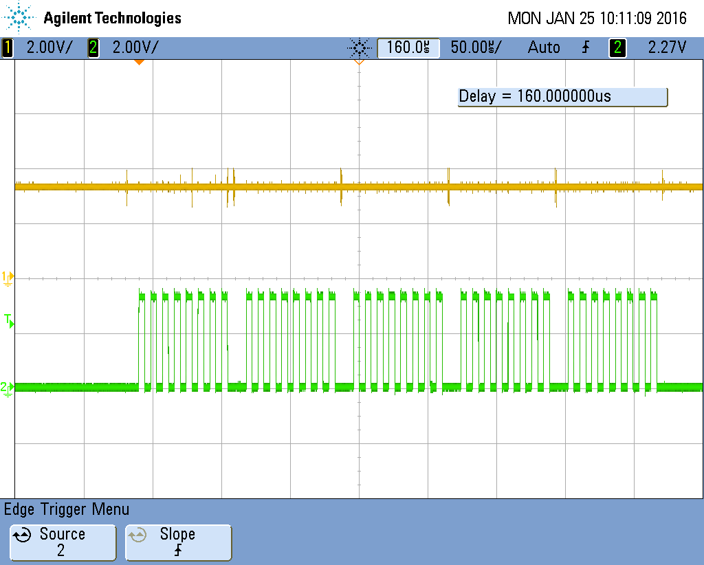
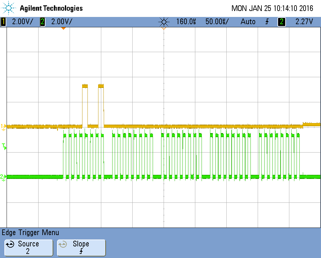
Device #1 has four independent pads for SPI - ~CS, SCLK, MOSI and MISO. This device works fine with the firmware.
Device #2 shares two out of four pads with TWI - namely, SCL/SCLK and SDA/MOSI; moreover, the ~CS pad is internally pulled up and should be driven LOW in order for the device to enter SPI mode. On that device, I keep on having the SDA/MOSI line at logic HIGH, no matter what data I send to the device. This results in getting 0xFF on the MISO line when I try to read data from the device.
I have been searching through this forum all day long and I have found the following post that resembles, to some extent, my case: SSI interface with accelerometer(H3LIS331DL). It states something about locked MCU pins and that was indicated as a solution to this problem. However, by browsing quickly through the MCU datasheet, I could not find anything relevant to that issue.
Does anyone have any idea on how can I get device #2 - that is otherwise functional, I repeat - to work on my test rig? Your answers are most welcome.