This thread has been locked.

If you have a related question, please click the "Ask a related question" button in the top right corner. The newly created question will be automatically linked to this question.

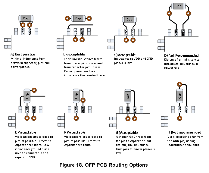
Confused decoupling technics for TM4C in System Design Guidelines for Tiva C family

It's about  System Design Guidelines for the TM4C129x Family

Confusing moment at page 20, Figure 18

Authors say what best practice is A (capacitor places outside trace )

But in other literature and guides best practice is such placement when capacitor places between via to power plane and MCU pin and trace is short is possible. Example:

As I know it's a common practice.

There are the reasons for such placement (as on Picture A) in case of Tiva C?

  • Hello Danil,

    The one that you have shown is a preferred method due to the low Trace resistance from the Cap to the Pins of the device. However the one shown in TM4C System Design Guidelines would work equally well. Note that the number of VDD pins on the device is significantly greater, so the trace impedance will have minimal effect.

    Regards
    Amit
  • Hello Amit!

    Thanks to your answer!
  • Hello Danil

    Just to elaborate. I have used method A, C and the method that you have highlighted. For me, it is based on the congestion during routing, that makes me change the scheme

    Regards
    Amit
  • Believe that poster Danil deserves praise for the care & concern displayed - especially his, "Attention to detail" wrt MCU board layout.

    That said - so often my small firm (and multiple clients) have found it advantageous to employ vendor's board as the MCU "base" - and confine their efforts to the design & production of plug-in, "accessory" boards - which best fulfill your (unique) application requirement.   This method proves far faster - more robust - and better accommodates the inevitable (change) which your design is (almost) sure to encounter.

    When the design is proven sound - and very much along - (then) often proves the best and (only) time to reduce multiple boards to just one - and place all of the MCU layout techniques into practice.   

    As one poster notes, (he knows who he is) "Premature optimization" is the (root) of much heartbreak - and some evil...

  • Hello cb1,

    I believe you are speaking on the lines of SoM boards, to minimize effort and maximize efficiency.

    Regards
    Amit
  • Hi Amit,

    Indeed that's one technique - yet more broadly - and repeatedly - we visit clients who've "spun their own" MCU boards - and failed.

    It is unlikely that small firms - and especially individuals - prove skilled/experienced enough to grasp the (many) nuances of fine-pitch IC layout, routing & component placement. Eval boards which "attach" to user's "accessory/custom" boards most always lead to a faster & less painful project solution.

    At that stage - and that stage only - are many(most) clients able to tackle the, "Single, custom, MCU & friends pcb design." (maybe!)

    From my read/review (this thread) poster IS qualified, aware, and proves, "Willing to sweat the details!"   Experience teaches that this is rare - and kidz should NOT, "Try this at home."

  • Hello cb1,

    Like you, I also have a small company for the development of hardware. I wrote this post is not because I do not know about the placement of decoupling capacitors, but because one of the engineers (embedded software division) saw the picture and asked - why is it the best practice for this MCU?

    My colleagues and I are very much surprised that such placement of the capacitor is "best practice". We would say the proposed "best practice" is a "acceptable practice". But not considering themselves the most intelligent, we decided to find out the reasons for this approach on forum=))

    "Premature optimization is the root of much heartbreak" - we fully support!

  • Hello Danil and cb1

    This is by far one of the most technically cordial conversation on the forum(s) that I have seen. There is a plan to start work on SoM boards for different packages and device family within TM4C12x to reduce effort and maximize operational efficiency. Of course no document is perfect, but the inputs we get on the forum brings us an inch closer progressively.

    Regards
    Amit
  • Thank for reply and elaborate!
  • Danil Borchevkin said:
    ...not considering themselves the most intelligent...

    May I note that, "accepting & embracing" that consideration (amost) "flies in the face" of that quote.   (i.e. it requires intelligence to know (and accept) that you/I, Do NOT know!)

    Past U.S. Gov't official stated, "There are (both) Known Unknowns and Unknown Unknowns!"   Those "unknown" ones - especially when arriving late in the project/process - prove especially unpleasant.  

    Being "open" to the fact that learning & understanding are never (really) "complete" (may) enable earlier & superior detection of the dreaded, "Unknown unknowns!"