This thread has been locked.

If you have a related question, please click the "Ask a related question" button in the top right corner. The newly created question will be automatically linked to this question.

I2S Emulation using SPI (TIVA TM4C1294XL and PCM1807)

Other Parts Discussed in Thread: PCM1807

Hello everybody.

First I'd like to thanks everyone for the help in this forum. That's being really helpful.

I'm working with the TIVA TM4C1294XL. I ran the spi_master.c example code and modified it a little bit to fit for that TIVA. So now, I found this article explaining how to emulate I²S on TIVA TM4C123x (http://goo.gl/tmwjEu). For this, I'm using the PCM 1807 A/D converter http://goo.gl/xtdK90

So I was reading about I²S and the I²S bus specification says that I need at least three lines in order to make I²S happens:

1. Continuous Serial Clock 

2. Word Select

3. Serial Data.

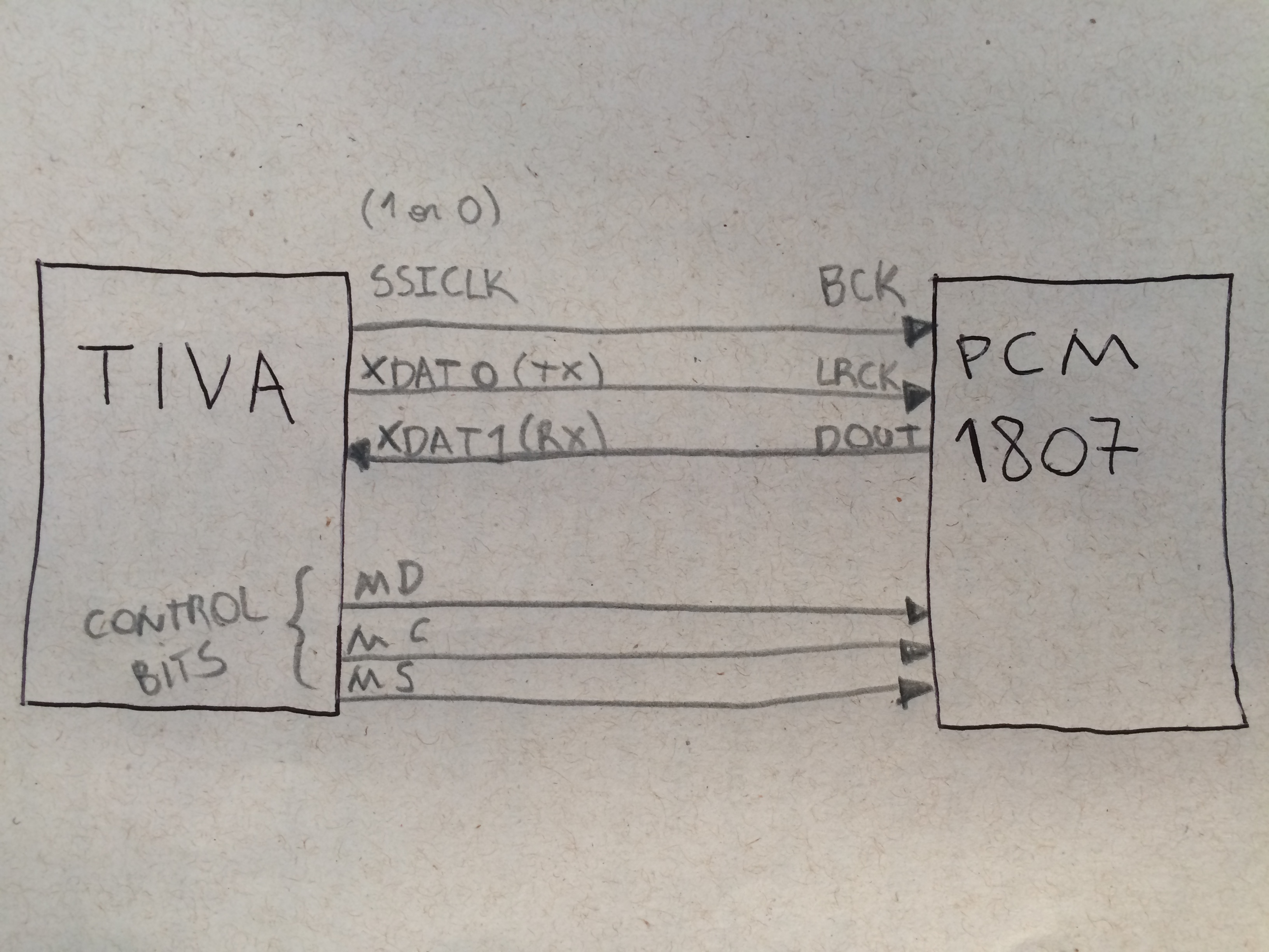
These three lines are drawn on page 2 of the first document. There I have SSI CLK hooked to BCLK, SSI TX hooked to DIN and SSI FSS hooked to WCLK, and another configuration lines for other purposes.

However, I want my TIVA to be the master, so I did this drawing (in advance apologies for the quality)

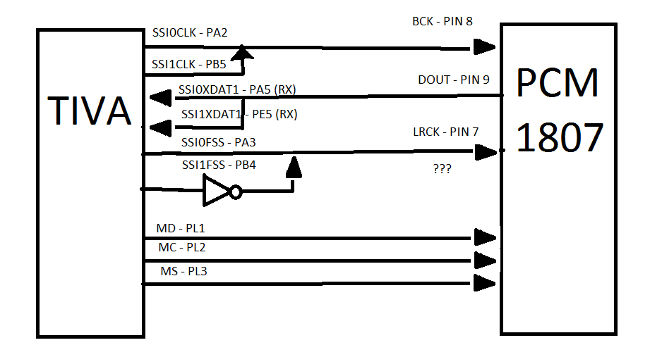
So I did that associations taking as example the I²S emulation on the first document. So my first question.

I believe I'd have a problem hooking SSI0CLK and SSI1CLK together, right? I mean, since the TIVA will dictate the CLK, I don't need both SSI0 and SSI1 to send clock, right? 

Another detail is that in the PCM 1807 datasheet, page 14, I have that if the PCM is working as SLAVE, LRCK and BCK are INPUT pins.But I believe that LRCK "says" right or left side, so that should be coming OUT of the ADC, or not?

For now, my last question is regarding the MC, MD and MS configuration pins. On the pages 22/23/24 of the ADC datasheet, I have the detailed explanation of how to work with MC, MD and MS in order to configure the ADC. So I planned to use three GPIOs from TIVA to set LOW and HIGH on MC, MD and MS. Considering correct previous PIN configuration, I did this:

uint32_t MD_bits[16];				//Control bits to Serial Control Format
uint32_t MC_bits[32];                           //Fake clock
uint32_t MS_bit = 0xff;
int i, j = 0;

//
// Initializing MD and MC arrays
//
MD_bits[16] = {0x00, 0x00, 0xff, 0xff, 0x00, 0x00, 0x00, 0xff, 0xff, 0xff, 0x00, 0x00, 0x00, 0x00, 0x00, 0x00};

for(i = 0; i < 32; i++){
    if(i%2 == 0)
    	MC_bits[i] = 0x00;
    else
   	MC_bits[i] = 0xff;
}

// Sending Serial Control Format - SPI

MS_bit = 0x00;								
GPIOPinWrite(GPIO_PORTL_BASE, GPIO_PIN_3, MS_bit); 			//Put MS to low to start transmitting MD and MC.

for(i = 0; i < 16; i++){
    GPIOPinWrite(GPIO_PORTL_BASE, GPIO_PIN_1, MD_bits[i]);  //Writes MD first
    GPIOPinWrite(GPIO_PORTL_BASE, GPIO_PIN_2, MC_bits[j]);  //Writes MC - Driven to LOW
    j++;                                                    //Increments j that is the MC counter since MC has twice MD's size
    SysCtlDelay(100);                                       //Waits 100 clock cycles
    GPIOPinWrite(GPIO_PORTL_BASE, GPIO_PIN_2, MC_bits[j]);  //Writes MC again - Driven to HIGH
    j++;													//Increments j again
    SysCtlDelay(100);                                       //Waits 100 more clock cycles
}

MS_bit = 0xff;
GPIOPinWrite(GPIO_PORTL_BASE, GPIO_PIN_3, MS_bit);			//Not necessary in the future

Would that work for this purpose? Or I can't use GPIO to write on MC, MD and MS?

I did a test last week and I got this (MC is wrong)

Thanks again!


Alex.

  • Should I2S be central to your design - would not (one of many) ARM MCUs "equipped w/a proper I2S peripheral module" prove far faster, easier & superior in performance?   As it stands now - you've bumped against much added "indirectness, delay & complexity" and your (compromised) end-results may not satisfy.  (likely will not) 

    Three-legged horses - even w/the best "kludged" saddles/shoes - are unlikely to perform well on the first Satuday in May - in Kentucky...

    Might mating a "proper tool" to the task warrant (some) consideration?

  • I might add that a 24-bit ADC is a real hardware design challenge. If the PCM1807 is not an imperative for your application, select another ADC (perhaps 16-bit resolution is sufficient), but with an interface directly supported by your TM4C MCU.

    Interface emulations are always third-best choice - the implementation can be complex and error-prone, while eating away core performance where you need it.

  • f. m. said:
    Interface emulations are always third-best choice

    Bravo - at least (two) now have noted this "emperor's" wardrobe as w/out full/proper accessories!   (my left eye stopped twitching - right still drips/drains...)

    Three-legged horse - Derby bound - is (more) likely, "Twenty-best choice."   (assumes 19 horses are, "in the field")

    Despite vendor's best, "bending, chiseling, welding" these "Franken-Chip" methods most always are sure to eat time/effort, raise hopes & then severely, "Disappoint!"

  • Hello f. m. and cb1_mobile, thanks for the answers!

    My whole project is just to create a "sound board". As an easy example, I want to hook a microphone to a 16-bits, 48 kHz ADC, transfer data through I²S to TIVA and transfer data from TIVA to a PC through USB.

    I got TIVA because it has many libraries - as they seems to be - easy to use. Also, what motivated me was the I²S emulation document I posted here.

    I'm still a bit confused about the PCM 1807. Even though it is a 24 bits ADC, I want to use only 16 - I mean, can I do that ?

    What would you all recommend for me to accomplish the mini project?

    Thanks again!!!! :)
  • I suggest a re-read of poster f.m.'s apt description of (any) vendor's attempt to "emulate" that which EXISTS upon (other, similar) MCUs.

    Libraries alone (and those here ARE good) cannot over-come less than inspired "Peripheral Inventory." (i.e. I2S, DAC - to name quick two...)
  • Hello Alex

    I think the I2S emulation document was targeted for TLV320AIC codec. Wouldn't it be more useful as well to use the known "good" setup to meet the requirements?

    Regards
    Amit
  • Hello all,

    I tried to use this configuration because at first glance it didn't seem impossible to do. My idea was understand SPI and replicate it twice to make I²S. 

    And to make I²S I meant configure TIVA GPIOs to send the data written on PCM 1807 datasheet and that was all. 

    So you're all saying that I WON'T be able to do that... why? Is not that simple as I think? 

    Changing the config will be the last option, because 1st - I couldn't find a simple configuration to do what I said before, and 2nd - I don't have that much money to spend (not counting that an item bought may take up to 1 month to get here in Brazil).

    I appreciate all your comments.

  • None here bear any responsibility for your predicament. Might it have been wise to ask here - before you made such purchase?
    As to simplicity - two "outsiders" have expressed their opinion. We're sorry if that displeases - yet it is steeped in experience & reality...
  • Hello Alex,

    Note that the original document uses TLV320AIC as the Audio Codec which has an IO configuration different from PCM1897 part. Secondly, the clock from TIVA are being wire-ANDED together. Not a good idea and neither is the wire AND of the two FSS signals (which are in opposite polarity). There is bus contention on two critical signals.

    Regards
    Amit
  • Hello Amit, thanks for the feedback.

    I was thinking in not using both clocks, since they'd be the same, right?

    "I believe I'd have a problem hooking SSI0CLK and SSI1CLK together, right? I mean, since the TIVA will dictate the CLK, I don't need both SSI0 and SSI1 to send clock, right? "

    However I'm not sure how I could handle the FSS signal. 

    "Another detail is that in the PCM 1807 datasheet, page 14, I have that if the PCM is working as SLAVE, LRCK and BCK are INPUT pins. But I believe that LRCK "says" right or left side, so that should be coming OUT of the ADC, or not?"

    Thanks!

  • Hello Alex,

    One solution would be to use the Bi-Write mode. In this mode the SSICLK can remain the clock, XDAT0 becomes the LRCK and XDAT1 becomes the data. However this approach would require that the data being sent needs to be processed by the micro. As an example if you wanted to send data "4'b1111" serially, then when sending with LRCK low you would need to write "8'b10101010" so that the even bits go to XDAT0 for LRCK and odd bits go to XDAT1 as the data.

    Regards
    Amit
  • Hello Amit - Thanks again for the feedback.

    So with this configuration (Bi-Write mode), I won't need both SSI0 and SSI1 to work, since I'll use SSI0CLK for clock, SSI0XDAT0 (TX) for LRCK and SSIXDAT1 (RX) for DOUT - I think.

    However, you said if I wanted to *send* data, but I'd be *receiving* data, right? Or you mean that SSI0XDAT0 and SSI0XDAT1 won't be in Legacy mode -  then working as Bi-directional data?

    Also, I have a question about ADCs. If the PCM has 24 bits of resolution, it means that 24 bits will be going out of DOUT when there's an analog input? If so, using XDAT0 and XDAT1 I'll be able to get only 8 bits, or not?

    Thanks again Amit.

  • Hello Alex,

    Looking at the design and knowing that the max length of DSS is 16 bits, yes, it should be in steps of 8.

    Regards
    Amit
  • A 24 bit device (likely upon a breadboard) and (just) emulated I2S - "concert-hall realism" (somehow) seems (not) in poster's future...

    Fifteen "back-forth" posts in - and not one byte transferred - not one! Is the slaughter rule ever appropriate?
  • Hello cb1_mobile,

    I'm sorry but I can barely understand what you're saying. I'm not an English native speaker neither a specialist in microcontrollers or electronics. Also, I have a very limited access to labs here - That's why I try to sane all my doubts before test something. 

    Thanks for the feedback.

    Alex.

  • My friend,

    Several times here it's been suggested that (any) 24 bit device requires VERY special care & handling - these (almost never) succeed when used in an early (especially a FIRST) project.

    It has also been noted that vendor's MCU is NOT best/brightest in terms of "I2S." Any "emulation" adds complexity, time, effort - and the end result is (always) less than that obtained from a proper MCU's (real) I2S peripheral.

    Thus - your choice of project is extremely complex - will be greatly taxing - and "if/when" you are fortunate enough to complete it - your results are unlikely to well satisfy!

    Might a "simpler" project (in agreement w/KISS [climb a small mountain first]) be a better means to build your skill & understanding?

    It is not the intent of poster f.m. or myself to be "mean" - instead we are suggesting that a more "realizable project" be chosen. (i.e. simpler and one which the MCU can (natively) support - not "emulate.")

    Few explorers or climbers "start" at Mt. Kilimanjaro - there's a reason for that - don't you agree?
  • Hello cb1_mobile.

    Now I understand. I believe that, that kind of emulation would take so much time for me to figure out - or even I wouldn't be able to do.

    What I'm planning then, is working with SPI to transfer data. However - a question that still needs answer for my head is:

    I have a 24-bits ADC. Is it UP TO 24 bits? I mean - can I work with a lower resolution to work with SPI? Or I would need a 16-bits ADC or even 12-bits ADC?

    My idea for understanding all these is just transfer whataver data from ADC to TIVA - regardless what kind of protocol/way/etc. Would that be possible somehow still using PCM1807 or it's still impossible because it's a 24-bits ADC?

    Thanks for all feedback.
    (Surely I don't think any of you all is being mean - I apologize if I meant that :) )
  • Thank you - any 24 bit ADC is highly specialized and most always must be placed upon a (very) carefully designed pcb. (even those w/many years in this field - often are forced to "several" pcb "spins.")

    If you can relax your ADC resolution from the (likely) unachievable 24 bits - to 12 - that resolution is natively supported w/in TM4C. Thus you comply w/KISS - and eliminate the requirement for SPI, external HW and its code demands.

    I2S peripherals exist as most emulations cannot really meet requirements - bloat code - and add time, cost & effort to the I2S design. I suspect poster f.m. and I (and others, fair-minded here) would agree that I2S is "far" from an ideal "first project" for you (and many others!)
  • Hello cb1_mobile,

    Thanks for the explanation! Regarding the use of TIVA's internal ADC - I will do it. However, I still want to try something with an external ADC, at least try.

    I believe that the use of TIVA's ADC is fairly "simple" compared to any external peripheral - that's why I still want to put some effort on using PCM 1807. That's why I asked if I can make PCM gives me 12 bits or if it's 24 bits and that's all.

    If the answer for the question is YES - you can work with 12 bits - I'd ask: Do you think it is worth trying to use SPI to work that way? Or it's still tough to make something work within a week or so?

    Thanks again for the tips! I really appreciate them :)

    Alex.
  • While your heart remains "set" on PCM1807 - I'd bet money that it will be broken - if you don't switch to a simpler device. The complexity of that device may be so demanding as to spoil your efforts - note "how far" you've progressed - thus far.

    Even a 14 or 16 bit ADC demands proper board & layout - but (again) w/a week remaining - even their use is risky.

    My small firm - when challenged by a "drop-dead" ship date - targets (always & only) the BASICS - and only when those are ALL achieved (meaning comprehensively test/verified) might we venture to the "extras."

    Your method, "Still climb Kilimanjaro" may result in (not even) the successful climb of a small hill. Not much more to say - bon chance mon ami.