


Hi all,
We have just done EMIF performance measurements with one Hercules Dev KIT with a Rev B mask (chip is marked "TMP570 4357BZW"). These measures
were done for asynchronous interface mode. We were happy to see that problems traced by errata #39 on Rev A mask is fully corrected for read cycles.
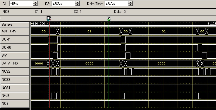
But for write cycles, we still have three WE pulses whatever the write type is (32 bits, 16 bits, 8 bits). This is exactly what was decribed in the forum subject "TMS570LC4357 Errata #39 clarification" where precise timing diagrams for 32/16/8 bits reads & writes were given by TI
By searching in forum we found that the problem may be due to incorrect programming of R5 core memory protection unit (MPU). So we did again the test by enabling the R5 core MPU and setting up a region for EMIF bus async (CS2, CS3, CS4) in "DEVICE" mode but we found no difference, problem was still present. We also did the same test with MPU region for EMIF bus async set to "STRONGLY_ORDERED" and we get the same problem (see joined figure). The programming of R5 core MPU is given in file also shown below (derived from same name file generated by HalCoGen)
So my question is to know if this errata of TMS570LC4357 still exists for writes cycles because the Rev B mask errata list (document spnz232 dated August 2015) indicates this Errata #39 has been corrected in Rev B mask, and it seems that there is no new errata dealing with EMIF bus in asynchronous mode for this new mask release.
This problem on write cycles leads to divide EMIF performance by a factor of 3 since for a simple 16 bits write, it takes 3 basic cycles instead of one. For instantaneous write performance, it's a problem in our real time application.
Thank you for your help
Best regards
Sylvain Balssa
-------------------- HL_sys_mpu.asm file (extract) -------------------------------
FLASHBase     .word 0x00000000
SRAMBase      .word 0x08000000
SYSPCR1Base   .word 0xFFF80000
SYSPCR2Base   .word 0xFC000000
SYSPCR3Base   .word 0xFF000000
TIOTPBase     .word 0xF0080000
EMIFASYNCBase .word 0x60000000
r7Base  	  .word 0x08000000
r8Base  	  .word 0x08000000
r9Base  	  .word 0x08070000
r10Base  	  .word 0x08070000
r11Base  	  .word 0x00000000
r12Base  	  .word 0x00000000
r13Base  	  .word 0xF0000000
r14Base  	  .word 0xF8000000
r15Base  	  .word 0xF8000000
r16Base  	  .word 0xF0000000

MPU_S_U_X     .equ 0x0000
MPU_SRW_U_X   .equ 0x0100
MPU_SRW_UR_X  .equ 0x0200
MPU_SRW_URW_X .equ 0x0300
MPU_SR_U_X    .equ 0x0500
MPU_SR_UR_X   .equ 0x0600
MPU_S_U_      .equ 0x1000
MPU_SRW_U_    .equ 0x1100
MPU_SRW_UR_   .equ 0x1200
MPU_SRW_URW_  .equ 0x1300
MPU_SR_U_     .equ 0x1500
MPU_SR_UR_    .equ 0x1600

MEMTYPE_STRONGLY_ORDERED .equ 000000B
MEMTYPE_SHAREABLE_DEVICE .equ 000001B
MEMTYPE_NORMAL_NON_CACHE .equ 001000B

MPU_SIZE_32B  .equ (00100B << 1)
MPU_SIZE_64B  .equ (00101B << 1)
MPU_SIZE_128B .equ (00110B << 1)
MPU_SIZE_256B .equ (00111B << 1)
MPU_SIZE_512B .equ (01000B << 1)
MPU_SIZE_1K   .equ (01001B << 1)
MPU_SIZE_2K   .equ (01010B << 1)
MPU_SIZE_4K   .equ (01011B << 1)
MPU_SIZE_8K   .equ (01100B << 1)
MPU_SIZE_16K  .equ (01101B << 1)
MPU_SIZE_32K  .equ (01110B << 1)
MPU_SIZE_64K  .equ (01111B << 1)
MPU_SIZE_128K .equ (10000B << 1)
MPU_SIZE_256K .equ (10001B << 1)
MPU_SIZE_512K .equ (10010B << 1)
MPU_SIZE_1M   .equ (10011B << 1)
MPU_SIZE_2M   .equ (10100B << 1)
MPU_SIZE_4M   .equ (10101B << 1)
MPU_SIZE_8M   .equ (10110B << 1)
MPU_SIZE_16M  .equ (10111B << 1)
MPU_SIZE_32M  .equ (11000B << 1)
MPU_SIZE_64M  .equ (11001B << 1)
MPU_SIZE_128M .equ (11010B << 1)
MPU_SIZE_256M .equ (11011B << 1)
MPU_SIZE_512M .equ (11100B << 1)
MPU_SIZE_1G   .equ (11101B << 1)
MPU_SIZE_2G   .equ (11110B << 1)
MPU_SIZE_4G   .equ (11111B << 1)

MPU_ENA_REGION   .equ (0x0001)
MPU_DIS_SUBREG1  .equ (0x1 << 8)
MPU_DIS_SUBREG2  .equ (0x1 << 9)
MPU_DIS_SUBREG3  .equ (0x1 << 10)
MPU_DIS_SUBREG4  .equ (0x1 << 11)
MPU_DIS_SUBREG5  .equ (0x1 << 12)
MPU_DIS_SUBREG6  .equ (0x1 << 13)
MPU_DIS_SUBREG7  .equ (0x1 << 14)
MPU_DIS_SUBREG8  .equ (0x1 << 15)


    .def     _mpuInit_
    .asmfunc

* --------------------------------------------------------------------------- *
* This function initializes MPU regions :                                     *
* - Region 1 : Flash : 4MB   / SRW_URW_X Normal mode                          *
* - Region 2 : SRAM  : 512KB / SRW_URW Normal mode                            *
* - Region 3 : System and module under PCR1/PCR3 : 16MB / SRW_URW Normal mode *
* - Region 4 : module under PCR2 : 16MB / SRW_URW Normal mode                 *
* - Region 5 : TI OTP : 16KB / SR Normal mode                                 *
* - Region 6 : EMIF Asynchronous : 256 MB / SRW_URW Strongly ordered mode     *
* --------------------------------------------------------------------------- *

_mpuInit_
        stmfd sp!, {r0}

        ; Disable mpu
        mrc   p15, #0, r0, c1, c0, #0
        bic   r0,  r0, #1
        dsb
        mcr   p15, #0, r0, c1, c0, #0
        isb

		; Disable background region
        mrc   p15, #0, r0,      c1, c0, #0
        bic   r0,  r0, #0x20000
        mcr   p15, #0, r0,      c1, c0, #0

        ; Set-up region 1 : Flash Prom
		;---------------------------------------------------
		;  - base address = 0x00000000
		;  - access control :
		;		- Memory type	= Normal non cacheable
		;		- Sharing 		= Non Shared
		;		- access		= Supervisor R&W + User R&W + Execution allowed
		;  - Size & Enable
		;		- Size = 4 MBytes
		;		- Enabled = YES
		;		- Sub-regions = all enabled
        mov   r0,  #0
        mcr   p15, #0,    r0, c6, c2, #0
        ldr   r0,  FLASHBase
        mcr   p15, #0,    r0, c6, c1, #0
        mov   r0,  #MEMTYPE_NORMAL_NON_CACHE
        orr   r0,  r0,    #MPU_SRW_URW_X
        mcr   p15, #0,    r0, c6, c1, #4
        movw  r0,  #(MPU_SIZE_4M | MPU_ENA_REGION)
        mcr   p15, #0,    r0, c6, c1, #2

        ; Set-up region 2 : SRAM
		;---------------------------------------------------
		;  - base address = 0x08000000
		;  - access control :
		;		- Memory type	= Normal non cacheable
		;		- Sharing 		= Non Shared
		;		- access		= Supervisor R&W + User R&W
		;  - Size & Enable
		;		- Size = 512 KBytes
		;		- Enabled = YES
		;		- Sub-regions = all enabled
        mov   r0,  #1
        mcr   p15, #0,    r0, c6, c2, #0
        ldr   r0,  SRAMBase
        mcr   p15, #0,    r0, c6, c1, #0
        mov   r0,  #MEMTYPE_NORMAL_NON_CACHE
        orr   r0,  r0,    #MPU_SRW_URW_
        mcr   p15, #0,    r0, c6, c1, #4
        movw  r0,  #(MPU_SIZE_512K | MPU_ENA_REGION)
        mcr   p15, #0,    r0, c6, c1, #2

        ; Set-up region 3 : System and module under PCR1/PCR3
		;---------------------------------------------------
		;  - base address = 0xFF000000
		;  - access control :
		;		- Memory type	= Normal non cacheable
		;		- Sharing 		= Non Shared
		;		- access		= Supervisor R&W + User R&W
		;  - Size & Enable
		;		- Size = 16 MBytes
		;		- Enabled = YES
		;		- Sub-regions = all enabled
        mov   r0,  #2
        mcr   p15, #0,    r0, c6, c2, #0
        ldr   r0,  SYSPCR3Base
        mcr   p15, #0,    r0, c6, c1, #0
        mov   r0,  #MEMTYPE_NORMAL_NON_CACHE
        orr   r0,  r0,    #MPU_SRW_URW_
        mcr   p15, #0,    r0, c6, c1, #4
        movw  r0,  #(MPU_SIZE_16M | MPU_ENA_REGION)
        mcr   p15, #0,    r0, c6, c1, #2

        ; Set-up region 4 : module under PCR2
		;---------------------------------------------------
		;  - base address = 0xFC000000
		;  - access control :
		;		- Memory type	= Normal non cacheable
		;		- Sharing 		= Non Shared
		;		- access		= Supervisor R&W + User R&W
		;  - Size & Enable
		;		- Size = 16 MBytes
		;		- Enabled = YES
		;		- Sub-regions = all enabled
        mov   r0,  #3
        mcr   p15, #0,    r0, c6, c2, #0
        ldr   r0,  SYSPCR2Base
        mcr   p15, #0,    r0, c6, c1, #0
        mov   r0,  #MEMTYPE_NORMAL_NON_CACHE
        orr   r0,  r0,    #MPU_SRW_URW_
        mcr   p15, #0,    r0, c6, c1, #4
        movw  r0,  #(MPU_SIZE_16M | MPU_ENA_REGION)
        mcr   p15, #0,    r0, c6, c1, #2

        ; Setup region 5 : TI OTP : 16K / SR
		;---------------------------------------------------
		;  - base address = 0xFF000000
		;  - access control :
		;		- Memory type	= Normal non cacheable
		;		- Sharing 		= Non Shared
		;		- access		= Supervisor R
		;  - Size & Enable
		;		- Size = 16 KBytes
		;		- Enabled = YES
		;		- Sub-regions = all enabled
        mov   r0,  #4
        mcr   p15, #0,    r0, c6, c2, #0
        ldr   r0,  TIOTPBase
        mcr   p15, #0,    r0, c6, c1, #0
        mov   r0,  #MEMTYPE_NORMAL_NON_CACHE
        orr   r0,  r0,    #MPU_SR_U_
        mcr   p15, #0,    r0, c6, c1, #4
        movw  r0,  #(MPU_SIZE_16K | MPU_ENA_REGION)
        mcr   p15, #0,    r0, c6, c1, #2

        ; Set-up region 6 : EMIF bus in asynchronous mode
		;---------------------------------------------------
		;  - base address = 0x60000000
		;  - access control :
		;		- Memory type	= Strongly ordered
		;		- Sharing 		= no meaning, strongly ordered type is always shareable ?
		;		- access		= Supervisor R&W + User R&W
		;  - Size & Enable
		;		- Size = 256 MBytes
		;		- Enabled = YES
		;		- Sub-regions = 7 and 8 disabled
        mov   r0,  #5
        mcr   p15, #0,    r0, c6, c2, #0
        ldr   r0,  EMIFASYNCBase
        mcr   p15, #0,    r0, c6, c1, #0
        mov   r0,  #MEMTYPE_STRONGLY_ORDERED
        orr   r0,  r0,    #MPU_SRW_URW_
        mcr   p15, #0,    r0, c6, c1, #4
        movw  r0,  #(MPU_SIZE_256M | MPU_DIS_SUBREG7 | MPU_DIS_SUBREG8 | MPU_ENA_REGION)
        mcr   p15, #0,    r0, c6, c1, #2

		; Setup region 7 : disable
        mov   r0,  #6
        mcr   p15, #0,    r0, c6, c2, #0
        ldr   r0,  r7Base
        mcr   p15, #0,    r0, c6, c1, #0
        mov   r0,  #0x0002
        orr   r0,  r0,    #0x1300
        mcr   p15, #0,    r0, c6, c1, #4
        movw  r0,  #((0 << 15) + (0 << 14) + (0 << 13) + (0 << 12) + (0 << 11) + (0 << 10) + (0 <<  9) + (0 <<  8) + (0x12 << 1) + (0))
        mcr   p15, #0,    r0, c6, c1, #2

		; Setup region 8 : disable
        mov   r0,  #7
        mcr   p15, #0,    r0, c6, c2, #0
        ldr   r0,  r8Base
        mcr   p15, #0,    r0, c6, c1, #0
        mov   r0,  #0x0002
        orr   r0,  r0,    #0x1300
        mcr   p15, #0,    r0, c6, c1, #4
        movw  r0,  #((0 << 15) + (0 << 14) + (0 << 13) + (0 << 12) + (0 << 11) + (0 << 10) + (0 <<  9) + (0 <<  8) + (0x12 << 1) + (0))
        mcr   p15, #0,    r0, c6, c1, #2

		; Setup region 9 : disable
        mov   r0,  #8
        mcr   p15, #0,    r0, c6, c2, #0
        ldr   r0,  r9Base
        mcr   p15, #0,    r0, c6, c1, #0
        mov   r0,  #0x000C
        orr   r0,  r0,    #0x1200
        mcr   p15, #0,    r0, c6, c1, #4
        movw  r0,  #((0 << 15) + (1 << 14) + (1 << 13) + (1 << 12) + (1 << 11) + (1 << 10) + (1 <<  9) + (1 <<  8) + (0x0E << 1) + (0))
        mcr   p15, #0,    r0, c6, c1, #2

		; Setup region 10 : disable
        mov   r0,  #9
        mcr   p15, #0,    r0, c6, c2, #0
        ldr   r0,  r10Base
        mcr   p15, #0,    r0, c6, c1, #0
        mov   r0,  #0x000C
        orr   r0,  r0,    #0x1300
        mcr   p15, #0,    r0, c6, c1, #4
        movw  r0,  #((1 << 15) + (0 << 14) + (1 << 13) + (1 << 12) + (1 << 11) + (1 << 10) + (1 <<  9) + (1 <<  8) + (0x0F << 1) + (0))
        mcr   p15, #0,    r0, c6, c1, #2

		; Setup region 11 : disable
        mov   r0,  #10
        mcr   p15, #0,    r0, c6, c2, #0
        ldr   r0,  r11Base
        mcr   p15, #0,    r0, c6, c1, #0
        mov   r0,  #0x0008
        orr   r0,  r0,    #0x0600
        mcr   p15, #0,    r0, c6, c1, #4
        movw  r0,  #((0 << 15) + (0 << 14) + (0 << 13) + (0 << 12) + (0 << 11) + (0 << 10) + (0 <<  9) + (0 <<  8) + (0x15 << 1) + (0))
        mcr   p15, #0,    r0, c6, c1, #2

		; Setup region 12 : disable
        mov   r0,  #11
        mcr   p15, #0,    r0, c6, c2, #0
        ldr   r0,  r12Base
        mcr   p15, #0,    r0, c6, c1, #0
        mov   r0,  #0x0010
        orr   r0,  r0,    #0x1600
        mcr   p15, #0,    r0, c6, c1, #4
        movw  r0,  #((1 << 15) + (1 << 14) + (1 << 13) + (1 << 12) + (1 << 11) + (1 << 10) + (1 <<  9) + (1 <<  8) + (0x15 << 1) + (0))
        mcr   p15, #0,    r0, c6, c1, #2

		; Setup region 13 : disable
        mov   r0,  #12
        mcr   p15, #0,    r0, c6, c2, #0
        ldr   r0,  r13Base
        mcr   p15, #0,    r0, c6, c1, #0
        mov   r0,  #0x0010
        orr   r0,  r0,    #0x1600
        mcr   p15, #0,    r0, c6, c1, #4
        movw  r0,  #((1 << 15) + (1 << 14) + (0 << 13) + (0 << 12) + (0 << 11) + (0 << 10) + (0 <<  9) + (0 <<  8) + (0x16 << 1) + (0))
        mcr   p15, #0,    r0, c6, c1, #2

		; Setup region 14 : disable
        mov   r0,  #13
        mcr   p15, #0,    r0, c6, c2, #0
        ldr   r0,  r14Base
        mcr   p15, #0,    r0, c6, c1, #0
        mov   r0,  #0x0010
        orr   r0,  r0,    #0x1100
        mcr   p15, #0,    r0, c6, c1, #4
        movw  r0,  #((0 << 15) + (0 << 14) + (1 << 13) + (0 << 12) + (0 << 11) + (0 << 10) + (1 <<  9) + (1 <<  8) + (0x1A << 1) + (0))
        mcr   p15, #0,    r0, c6, c1, #2

		; Setup region 15 : disable
        mov   r0,  #14
        mcr   p15, #0,    r0, c6, c2, #0
        ldr   r0,  r15Base
        mcr   p15, #0,    r0, c6, c1, #0
        mov   r0,  #0x0010
        orr   r0,  r0,    #0x1300
        mcr   p15, #0,    r0, c6, c1, #4
        movw  r0,  #((0 << 15) + (0 << 14) + (1 << 13) + (0 << 12) + (0 << 11) + (0 << 10) + (1 <<  9) + (1 <<  8) + (0x1A << 1) + (0))
        mcr   p15, #0,    r0, c6, c1, #2

		; Setup region 16 : disable
        mov   r0,  #15
        mcr   p15, #0,    r0, c6, c2, #0
        ldr   r0,  r16Base
        mcr   p15, #0,    r0, c6, c1, #0
        mov   r0,  #0x0000
        orr   r0,  r0,    #0x1300
        mcr   p15, #0,    r0, c6, c1, #4
        movw  r0,  #((0 << 15) + (0 << 14) + (0 << 13) + (0 << 12) + (0 << 11) + (0 << 10) + (0 <<  9) + (0 <<  8) + (0x1B << 1) + (0))
        mcr   p15, #0,    r0, c6, c1, #2

        ; Enable mpu
        mrc   p15, #0, r0, c1, c0, #0
        orr   r0,  r0, #1
        dsb
        mcr   p15, #0, r0, c1, c0, #0
        isb
        ldmfd sp!, {r0}
        bx    lr

    .endasmfunc
;-------------------------------------------------------------------------------

